Exclusive Interview: Nobel Prize and Global Energy Prize Winner Prof. Shuji Nakamura
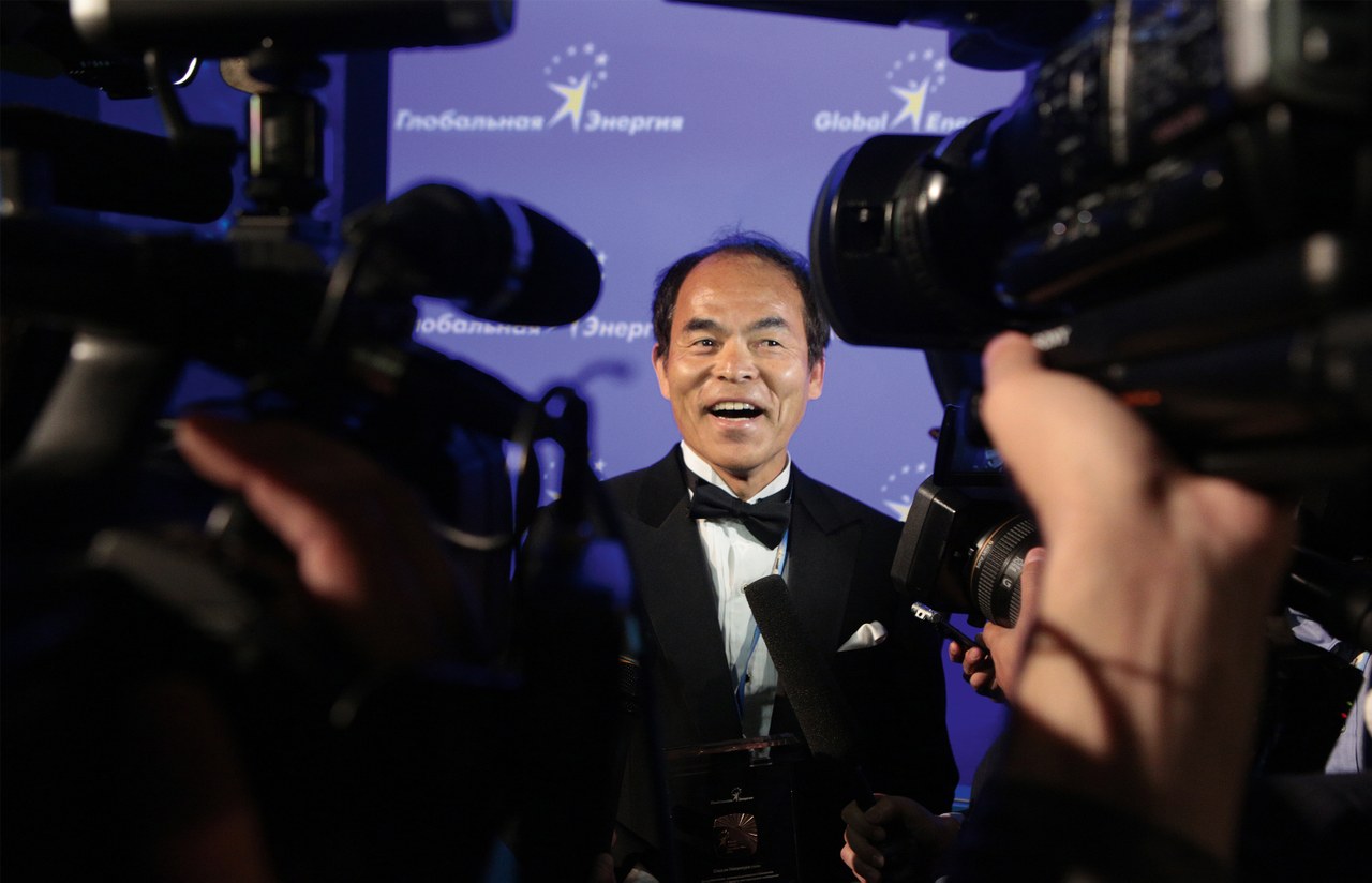
On June 19th, 2015 Nobel and Millennium prize winner, Professor Shuji Nakamura was awarded the Global Energy Prize in St. Petersburg, Russia. The Global Energy Prize is given to researchers in the field of energy efficiency and renewable technologies on a global scale. During the Global Energy Prize Event in St. Petersburg, Professor Nakamura gave an exclusive interview about the developments and future of solid-state lighting. Siegfried Luger, CEO of Luger Research, Event Director of the LpS 2015 and Publisher of LED professional, talked with Professor Nakamura about LED substrate technologies, violet and ultra-violet emitters, nano-technologies, OLEDs and laser technologies.

LED professional: It’s a great pleasure and honor to have this opportunity to talk with you about solid-state lighting here in St. Petersburg on the occasion of the Global Energy Prize event. If you don’t mind, I would like to start with a question related to LED substrate technologies. After your invention of the blue and white LEDs, you started doing research on GaN-on-GaN technology at the University of California Santa Barbara (USCB). When was this exactly?
Professor Nakamura: I moved to USCB as a professor in the Material Department in the year 2000. And that’s when we started to do research on GaN-on-GaN technology. At that time, nobody did work on GaN-on-GaN.
LED professional: What are the major advantages of GaN-on-GaN technology in comparison to other basic LED substrate technologies?
Professor Nakamura: Basically, the dislocation effects are much lower with GaN-on-GaN technology because the substrate is the same material as the epitaxial growth material. The lattice mismatch for GaN-on-Sapphire technology is much higher because the atomic arrangement is different. On the interface between Sapphire and GaN there are a huge number of dislocations with a density of approximately 109 cm-2. These dislocations basically cause non-radiation effects because the electrons in the InGaN layer are captured in the dislocations instead of recombining and the emission gets low especially at high current densities. On the other hand, with GaN-on-GaN technology the recombination works efficiently due to minimized dislocations and, in addition, thermal stress is also minimized.

Figure 1: Prof. Shuji Nakamura and Siegfried Luger met in St. Petersburg in advance of the Global Energy Prize award ceremony for an exclusive interview
LED professional: Does this lead to higher efficacy values when using GaN-on-GaN substrate technology instead of GaN-on- Sapphire technology, for example?
Professor Nakamura: Yes, this is especially the case at higher current densities because those undesirable recombinations caused by crystal dislocations are very active at high current densities. We founded a company named Soraa in 2008, which is using GaN-on-GaN technology. Soraa started the commercialization of GaN-on-GaN technology, and, hence, GaN-on-GaN LEDs. These products use between 5 to 10 times higher current densities, with up to 1000 Acm-2, as conventional LEDs on Sapphire based devices.
LED professional: But what about the droop effect with the GaN-on- GaN technology at such high current densities?
Professor Nakamura: The current droop effect is especially composed of Auger recombination with a contribution of about 50%. The other 50% comes from carrier overflow and dislocation. The droop effect with GaN-on-GaN is small because of the elimination of dislocations. With foreign substrate materials the droop effect is in the region of minus 18% to 27% while GaN-on-GaN technology shows just about minus 4%. Also with violet LEDs the droop effect is smaller than with blue LEDs.
LED professional: Another substrate technology is GaN-on- Silicon. How do you see this technology, which is also especially driven to reduce the future costs of the devices?
Professor Nakamura: GaN-on- Silicon dislocation is similar to GaN-on-Sapphire and the thermal mismatch is very high. The process of manufacturing GaN-on-Silicon LEDs is very complicated because it is necessary to insert additional layers to minimize the stress effects and the yield is very poor.
LED professional: To conclude the discussion about the substrate material: Which material will be the winner at the end of the developments?
Professor Nakamura: GaN-on-GaN technology will be the winner in the future. Just think of same size chips. The GaN-on-GaN chip would be five times brighter than chips based on other technologies. This means for the same light output we could reduce the chip size of a GaN-on- GaN based substrate chip to one-fifth of the size of a conventional LED chip because the current is five times higher. The substrate is expensive but for an LED bulb, for example, the substrate contributes with just about 10 to 13 % of the total costs.
LED professional: With such high current densities and brightness per single light point the glare problem might become much more important in applications. How do you see these visual effects and how can we solve these problems?
Professor Nakamura: For lighting designs you just need a point light source because then it is easy to control the light by just using a lens. With a lens you can do any kind of light distribution. To use a single lens approach we need a very tiny chip, which is the case with the GaN-on-GaN technology. A point light source based on a tiny chip is the principal used to help reduce the system costs because elements such as optics and cooling devices can be minimized.
LED professional: Are there any bottlenecks for mass production for the GaN-on-GaN technology when considering high-volume manufacturing?
Professor Nakamura: Right now GaN substrate is growing by hydride vapor-phase epitaxial (HVPE) growth, which is an expensive production process. We do research to reduce the cost of GaN substrate production further. So right now, we are doing research with ammono-thermal GaN crystal growth methods, which will be ready for mass-production for 4-, 6- and 8-inch GaN wafers in about 3 to 5 years. The research team is also testing growing GaN on different crystal planes to create semi-polar LEDs to drive down costs.
LED professional: You did a lot of research with different wavelengths as a primary source from the blue to violet up to ultra-violet bandwidths. What is the best choice for generating white light systems?
Professor Nakamura: UV LEDs were not planned to use for lighting. UV LEDs are for instance used in water purification or curing applications. Overall, the violet bandwidth is the best choice when you take the Stoke’s shift losses, color rendering and the excitation of materials like fluorescents into account. For example, blue LEDs have wall-plug efficiencies between 50 and 60% but with the violet GaN-on-GaN technology the wall-plug efficiency is about 80%, which is world record. But taking the Stoke’s shift into account for the shorter wavelength of the violet, then both systems are similar in efficiency but the difference is for the CRI value. Emitting in the violet bandwidth the CRI is more than 95 where in comparison the blue LEDs are typically at 85 CRI. With violet systems, having a full-spectra light, we can almost copy sunlight.
LED professional: Let’s talk about the laser technology for generating white light, which is currently used as a high beam booster in headlamps for the high-class cars, Audi R8 and BMWi8. Is this also a technology for general lighting applications in the future?
Professor Nakamura: The first generation to produce white light was the blue LED technology. The second generation of white light sources is the violet GaN-on-GaN technology and the third generation is laser technology. For blue LEDs the current densities are just around 10 Acm-2 with a huge droop effect. For violet LEDs we reach about 50-100 Acm-2 but the laser diode uses 3-10 kAcm-2 which is about 1,000 times higher than blue LEDs. This leads to very tiny chips in combination with the same phosphors such as YAG types. The light output is about 1,000 times higher than conventional LEDs with the same chip-size.

Figure 3: For the Celebration Issue 50, Prof. Nakamura and Siegfried Luger discussed the future of Solid-State Lighting from substrates to applications
LED professional: So, are you saying that laser technology is the third generation and that in maybe a decade, this technology will replace all other ones for generating white light?
Professor Nakamura: Yes, in about 10 years all white light systems will become laser-based lighting and the blue LEDs will be replaced completely. Think of a reduction in chip-size by a factor of 1,000. In terms of thermal management it will be easy because the chip-size is very small. Also, we can reach up to 90% of wall plug efficiencies with laser-diodes in the future. This technology will be ready in 5 to 10 years because we see existing applications in the automotive industry right now. By then it will also be used for general lighting. Just think of this meeting room here: One tiny chip based on laser technology will be enough to illuminate the whole room. It’s easy to distribute the light based on a very tiny point light source. We could not reach this with blue LEDs.
LED professional: What type of research are you doing in laser technology right now?
Professor Nakamura: In 2008 we founded two companies. One is Soraa, which focuses on LED lighting especially the GaN-on-GaN violet LEDs. Kaai focused on laser technology for lighting applications. After a merging of these companies we split them again and the laser part is now called Soraa Laser Diode. The development of laser lighting takes time for two reasons: The wall-plug efficiency is at 30% at the moment, so about half of the blue LED values. We have to increase that to reach more than 50, 60 or even 70%. The other problem is the costs because the laser diodes are expensive. They are about 10 times more than conventional LEDs. To overcome this we have to increase the yield and find solutions for any kind of process problems. However, we are very optimistic that we can solve these problems for this new technology.
LED professional: So that is a clear view on the future development steps for white light generation from blue LEDs to violet LEDs and finally to Laser lighting. But how do you see the developments in Nano-technologies?
Professor Nakamura: I saw results of red and green laser diodes with Nano-wired technologies. It is a great technology. I like the phosphor concept to make white light because we need broad spectra, like sunlight. With specific Nano- spectra we are missing colors and therefore, for me, phosphor is the best concept to generate white light and it can be used for all white light technologies. The human friendliest light is sunlight. It is the best for the human eye and so we have to copy sunlight to reach a full
spectra and to prevent missing colors.
LED professional: Another technology, which has been developed over the last years are OLEDs. Do you see OLEDs for general lighting applications as an alternative technology to your shown three generations SSL roadmap?
Professor Nakamura: For lighting applications I don’t see a way with OLEDs. I think it is too late because with existing LEDs you also can produce flexible lighting systems. The advantage of OLEDs is that they can be very thin for flat designs. But we also can make the same type of designs with LED lighting. And OLED lighting still has problems with reliability and costs.
LED professional: What are the TOP-three research fields, or let us say challenges, for white light system developments?
Professor Nakamura: On a chip level we have the current droop problem to solve, so droop is the biggest issue. For laser lighting we have no droop issues, so for me laser lighting is the perfect light source. On a chip level we can solve any kind of problems,
I think. On a system level the biggest issue is the heat sink and heat temperature increase. Also the laser lighting phosphor is a big challenge because the light output density is so high that with the same designs as for blue LEDs the phosphor would be burned down. For this reason they use a special remote ceramic phosphor in automotive applications.
LED professional: Professor Nakamura your research and inventions have a big influence on many areas in our lives and your contributions to environmental issues
are so big. The Nobel Prize and now the Global Energy Prize both confirm these contributions. How do you feel and what do you think when looking back at your research and your findings?
Professor Nakamura: Of course I’m very happy. But the Nobel Prize and the Global Energy Prize was given for the invention of the blue LEDs. But the second and third generation of lighting is required to improve lighting further. So in fact I’m happy, but it’s not good enough!
Prof. Shuji Nakamura
Shuji Nakamura was born on May 22, 1954, in Ehime, Japan. He received
his B.E., M.S., and Ph.D. degrees in electrical engineering from the University of Tokushima, Tokushima, Japan, in 1977, 1979, and 1994, respectively. He joined Nichia Chemical Industries Ltd., Tokushima, Japan, in 1979. In 1988, he spent a year at the University of Florida, Gainesville, FL, USA, as a Visiting Research Associate. In 1989, he started the research of blue LEDs using group-III nitride materials. In 1993 and 1995, he developed the first group-III nitride-based blue/green LEDs. He also developed the first group-III nitride-based violet laser diodes (LDs) in 1995. Since 2000, he has been a Professor at the Materials Department, University of California Santa Barbara, Santa Barbara, CA, USA. He holds more than 300 patents and has published more than 400 papers.
Dr. Nakamura has received a number of awards, including: The Nishina Memorial Award (1996), the MRS Medal Award (1997), the IEEE Jack A. Morton Award, the British Rank Prize (1998), and the Benjamin Franklin Medal Award (2002). He was elected a member of the U.S. National Academy of Engineering (NAE) in 2003. He received the Finnish Millennium Technology Prize in 2006. In 2008, he also received the prize of Asturias Award from Spain. He received the Harvey Prize of the Israel Institute of Technology in 2010. The 2014 Nobel Prize for physics has been awarded to a trio of scientists (Professors Isamu Akasaki, Hiroshi Amano and Shuji Nakamura) in Japan and the US for the invention of blue light emitting diodes. In June 2015 Professor Nakamura received the Global Energy Prize in St. Petersburg for the invention, commercialization and development of energy-efficient white lighting technology together with Jayant Baglia for the invention, development and commercialization of Insulated Gate Bipolar Transistor, which is one of the most important innovations for the control and distribution of energy.
