Business | Mar 14, 2023

Avicena Partners with ams OSRAM to Enable High-volume Future Production of Ultra-low Energy Chip-to-Chip Interconnects

AvicenaTech Corp., a privately held company in Sunnyvale, CA, has partnered with ams OSRAM to develop high-volume manufacturing of GaN microLED arrays for its industry-leading LightBundle™ communication architecture.

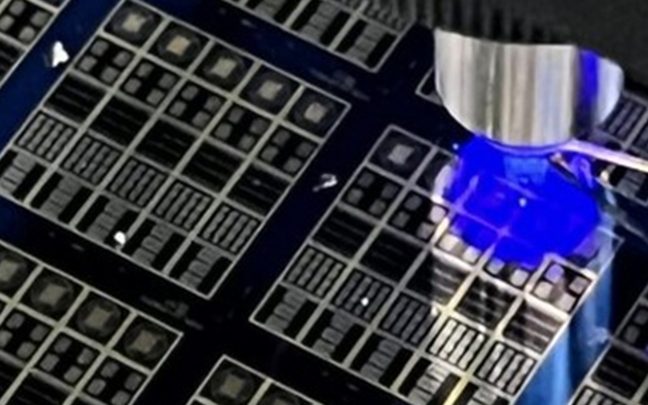
The need for next generation computing power is here, driven by strong AI/ML and HPC application demand – for products like ChatGPT, DALL-E, autonomous vehicle training, and many others.  Attempts to scale current architectures are running headlong into physical limits leading to slower throughput growth, power-hungry and hard to cool systems. The Avicena LightBundle architecture breaks new ground by unlocking the performance of xPUs, memory and sensors – removing key constraints of bandwidth and proximity while simultaneously offering an order-of-magnitude reduction in power consumption.

“Avicena’s LightBundle technology provides an opportunity for GaN microLEDs to impact numerous key applications including HPC, AI/ML, sensors, automotive and aerospace. As a global leader in GaN LEDs, we are excited to partner with Avicena to transform these very large and important markets.”

— ROBERT FEURLE, EXECUTIVE VICE PRESIDENT AND MANAGING DIRECTOR, OS BUSINESS UNIT AT AMS OSRAM

“We acquired our fab from Nanosys in October to accelerate our development efforts and support low-volume prototype manufacturing,” says Bardia Pezeshki, founder and CEO of Avicena. “However, we are addressing very sizeable markets requiring high-volume manufacturing. We are very pleased to partner with one of world’s top GaN LED companies to provide a path to satisfy the expected high volumes required by our customers, including hyperscale datacenter operators and the world’s leading IC companies.”

“Avicena’s LightBundle technology provides an opportunity for GaN microLEDs to impact numerous key applications including HPC, AI/ML, sensors, automotive and aerospace,” says Robert Feurle, Executive Vice President and Managing Director, OS Business Unit at ams OSRAM. “As a global leader in GaN LEDs, we are excited to partner with Avicena to transform these very large and important markets.”

About the Technology

Today’s high-performance ICs use SerDes-based electrical links to achieve adequate IO density. However, the power consumption and bandwidth density of these electrical links degrade quickly with length.  Conventional optical communications technologies developed for networking applications have been impractical for inter-processor and processor-memory interconnects due to their low bandwidth density, high power consumption, and high cost. Moreover, co-packaging existing laser sources with hot ASICs does not fit well for reliability reasons unless external laser sources (ELS) are used which increases complexity and cost.

Avicena’s LightBundle™ links use densely packed arrays of GaN microLEDs to create highly parallel optical interconnects with typical throughputs of > 1Tb/s at energies of < 1 pJ/bit. A LightBundle cable uses a highly multicore multimode fiber to connect a GaN microLED transmitter array to a matching array silicon photodetectors (PDs). Arrays of hundreds or thousands of LightBundle’s microLEDs and PDs are easily integrated with standard CMOS ICs, enabling the closest integration of optical interconnects with electrical circuits.  In addition to high energy efficiency and high bandwidth density, these LightBundle links also exhibit low latency since the modulation format of the individual links is simple NRZ instead of PAM4 which is common in many modern optical links but has the disadvantage of higher power consumption and additional latency.

The parallel nature of LightBundle is well matched to parallel chiplet interfaces like UCIe, OpenHBI, and BoW, and can also be used to extend the reach of compute interconnects like PCIe/CXL, HBM/DDR/GDDR memory links, as well as various inter-processor interconnects like NVLink with low power and low latency.

About Avicena

Avicena Tech Corp. is a privately held company located in Sunnyvale, CA, developing LightBundle, a next generation computing architecture for AI/ML, HPC, sensors, 5G wireless and aerospace applications.  This unique, flexible ultra-low energy technology is based on microLEDs, offering both very high bandwidth and low latency.  Now, system designers can disaggregate functions like compute and memory and radically grow system throughput.  Avicena’s technology is a key building block in the evolution of networking and computing that will reduce the energy impact on our planet.

For more information, visit https://avicena.tech


© 2023 Luger Research e.U. – Institute for Innovation & Technology

page_peel