Major Milestone Passed with Photonic Crystal Patterning on Full 4” Wafers
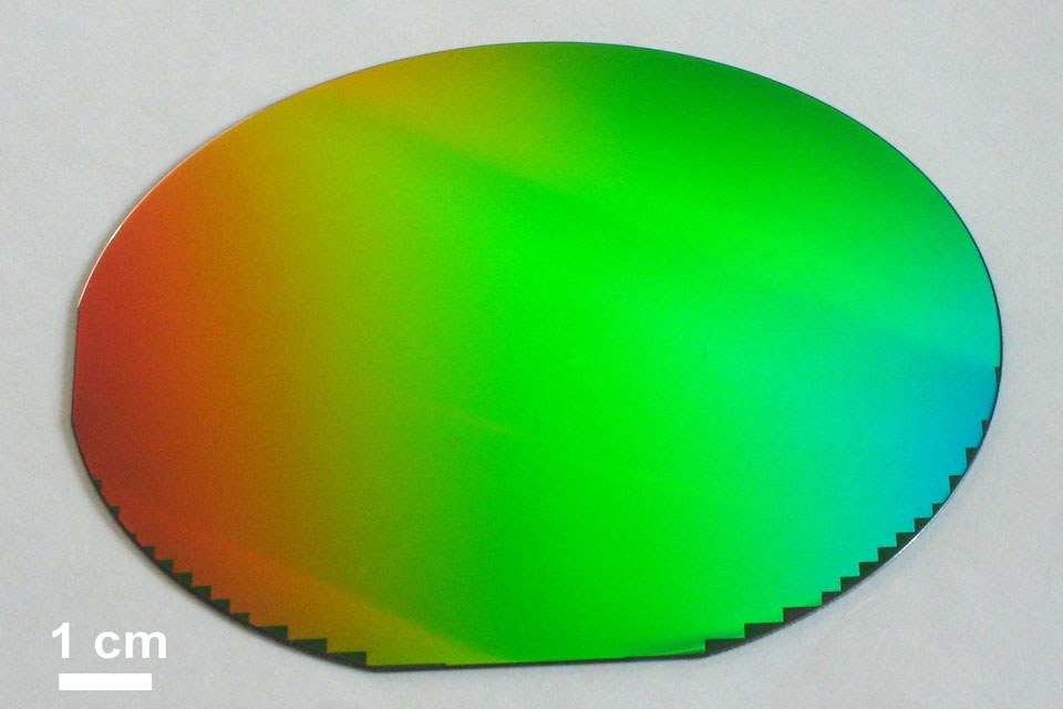
Eulitha AG of Switzerland and Dai Nippon Printing Co., Ltd. (DNP) of Japan announced the successful patterning of 4” wafers with Eulitha’s proprietary PHABLE technology. Photonic crystal patterns with 600 nm period and hexagonal symmetry was created uniformly over 4” wafers.

PHABLE (see also LED professional news from Oct 19, 2010) is a novel mask based photolithography technology that promises to revolutionize production of photonic structures such as photonic crystals, diffraction gratings and anti-reflection surfaces. High-throughput fabrication of such patterns over large areas is required for fabrication of high performance future devices in fields including LEDs, solar cells and flat-screen displays. In PHABLE a mask is illuminated with a UV beam to form a high resolution image that has a very large depth of focus. Therefore substrates with non flat surfaces can be patterned easily.
The necessary high-resolution mask with the same 4-inch area as the final pattern was produced by DNP on a standard quartz/Cr plate. UV photolithography exposures were performed on a PHABLE-R lithography tool made by Eulitha. Photonic crystal patterns consisting of circular holes on a 600-nm period hexagonal lattice were printed in a commercially available photoresist coated on Si wafers. The produced patterns were highly uniform over the whole 4” area of the wafers.
Demonstration of uniform patterning on 4” substrates is an important milestone as most targeted applications require patterning of large areas. For example, the high brightness LED industry is switching to 4” and 6” wafers from the traditional 2” base. Photonic crystal structures that enhance light extraction in LEDs or patterned sapphire substrates that improve performance of LEDs grown on them can be fabricated with the PHABLE technology. Similarly, the required substrates for nanowire based LED or solar cell applications can be produced with this technology.
Eulitha currently offers samples and wafer batch processing services to companies and researchers developing nanostructure-based products. It is also currently offering laboratory lithography tools for 2”-4” wafers that are suitable for product development.
About Eulitha AG:
Eulitha AG is a spin-off company of the Paul Scherrer Institute, Switzerland. It specializes in the development of lithographic technologies for applications in photonics, biotech, patterned magnetic media and EUV optics. It produces and markets nano-patterned samples and templates using its unique EUV interference method and state-of-the-art e-beam lithography tools. PHABLE is the brand name of its new photolithography platform, which includes exposure tools and wafer patterning services. For more information about Eulitha, please visit www.eulitha.com/
About DNP:
DNP is one of the world's largest comprehensive printing companies and conducts a wide range of businesses, including publication printing, commercial printing, smart cards, business forms, networking and electronic components. The company is the world’s leading supplier of high-tech photomasks, produced by applying fundamental printing techniques and technologies. For more information about DNP, please visit www.dnp.co.jp/index_e.html
