Organic light emitting diode (oled) having improved stability, luminance, and efficiency
An organic light emitting diode (OLED) includes a relatively thin diamnond-like carbon (DLC) layer disposed between the anode and the hole transport layer to improve luminous efficiency and operating life time. The relatively thin DLC layer inhibits hole injection, which balances charge flow and improves efficiency, and increases the surface smoothness of the anode, which contributes to the increased operating life time.
")
Background of the invention
[0002] In recent years, organic light-emitting diodes (OLEDs) have become increasingly important. This is due, at least in part, to the technological potential for OLED use in numerous products including, for example, multi-color, self-luminous flat-panel displays. An OLED exhibits several advantages over other light emitting devices. Some of these advantages include its wide range color emission capability, relatively low-voltage (e.g., <3V) operational capability, high-efficiency with low-power consumption, wide-viewing angle, and high-contrast.
[0003] A typical OLED includes an anode, a cathode, and at least two organic material layers disposed between the anode and cathode. The anode in many OLEDs comprises a relatively high work function material, such as indium tin oxide (ITO), and the cathode typically comprises a relatively low work function material, such as calcium (Ca). One of the organic material layers in a typical OLED comprises a material having the ability to transport holes, and is thus typically referred to as a hole transport layer. Another organic material layer typically comprises a material having the ability to transport electrons, and is thus typically referred to as an electron transport layer. The electron transport layer may also function as the luminescent medium (or emissive layer). Alternatively, an additional emissive layer may be disposed between the hole transport layer and the electron transport layer. In either case, when the OLED is properly biased, the anode injects holes (positive charge carriers) into the hole transport layer, and the cathode injects electrons into the electron transport layer. The injected holes and electrons each migrate toward the oppositely charged electrode. When an electron and hole localize on the same molecule, a Frenkel exciton is formed, and visible light is emitted.
[0004] While OLEDs have already appeared in some commercial applications, such as displays for mobile phones and digital cameras, certain challenges still remain to resolve various issues that adversely impact device reliability, chromaticity, and luminous efficiencies. For example, the surface roughness of anodes that comprise certain materials, such as indium tin oxide (ITO), contributes to the formation of dark spots, degradation, and eventual failure of many current OLEDs. As such, a significant amount of effort has been expended to improve OLED performance by modifying the anode surface. Some examples of anode surface modification techniques that have been attempted include chemical treatment, UV ozone treatment, oxygen plasma treatment, and mechanical polishing and annealing. In addition to these surface treatments, various other approaches have been attempted to address the adverse impact associated with anode surface roughness. These other approaches include depositing a layer of material, such as CuPc, LiF, Platinum, SiO.sub.2, metal oxide, or parylene, onto anode surface. Although such treatments and modifications may enhance hole injection from the ITO anode and improve the luminous efficiency of the OLED, these treatments and modifications do not sufficiently improve the life time of the OLED.
[0005] Hence, there is a need for an OLED that exhibits adequate performance, such as high luminous efficiency and long life time, so that OLEDs can be used in relatively high-demand applications. The present invention addresses at least this need.
Brief summary of the invention
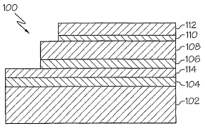
[0006] The present invention provides OLEDs having improved stability, luminance, and efficiency. In one embodiment, and by way of example only, an organic light emitting diode includes an anode, a diamond-like carbon (DLC) layer, an organic hole transport layer, an organic emission layer, and a cathode. The DLC layer is disposed on the anode, and has a thickness that is less than about 10 nm. The organic hole transport layer is disposed on the DLC layer, the organic emission layer is disposed on the hole transport layer, and the cathode is disposed on the organic emission layer.
[0007] In another exemplary embodiment, an organic light emitting diode includes a substrate, an anode, a tetrahedral amorphous carbon (ta-C) layer, an organic hole transport layer, an organic emission layer, and a cathode. The anode is disposed on the substrate, the ta-C layer is disposed on the anode, the organic hole transport layer is disposed on the ta-C layer, the organic emission layer is disposed on the hole transport layer, and the cathode is disposed on the organic emission layer.
Claims
1. An organic light emitting diode, comprising: an anode; a diamond-like carbon (DLC) layer disposed on the anode, the DLC layer having a thickness less than about 10 nm; an organic hole transport layer disposed on the DLC layer; an organic emission layer disposed on the hole transport layer; and a cathode disposed on the organic emission layer.
2. The OLED of claim 1, wherein the anode comprises indium-tin-oxide (ITO).
3. The OLED of claim 2, wherein the anode is about 60 nm in thickness.
4. The OLED of claim 1, wherein the anode comprises a material selected from the group consisting of indium-tin-oxide (ITO), metal doped zinc oxide (ZnO).
5. The OLED of claim 1, wherein the organic hole transport layer comprises polyethelen dioxy thiophene (PEDOT).
6. The OLED of claim 5, wherein the organic hole transport layer is about 20 nm in thickness.
7. The OLED of claim 1, wherein the organic hole transport layer comprises a water-soluble polymer.
8. The OLED of claim 1, wherein the organic emission layer comprises poly (p-phenylen vynelene) (PPV).
9. The OLED of claim 8, wherein the organic emission layer is about 90 nm in thickness.
10. The OLED of claim 1, wherein the organic emission layer is selected from the group consisting of poly (p-phenylen vynelene) (PPV) and polyfluorene (PFO) series materials.
11. The OLED of claim 1, wherein the cathode comprises calcium.
12. The OLED of claim 11, wherein the cathode is about 5 nm in thickness.
13. The OLED of claim 1, wherein the cathode is selected from the group consisting of calcium, lithium, natrium, kalium, Mg:Ag, Li:Al, Mg:Al, Ca:Ag, Ca:Al, Ba:Ag, and Ba--Al.
14. The OLED of claim 1, wherein the DLC layer thickness is less than about 1.0 nm.
15. The OLED of claim 1, wherein the DLC layer thickness is about 0.5 nm.
16. An organic light emitting diode, comprising: a substrate; an anode disposed on the substrate; a tetrahedral amorphous carbon (ta-C) layer disposed on the anode; an organic hole transport layer disposed on the ta-C layer; an organic emission layer disposed on the hole transport layer; and a cathode disposed on the organic emission layer.
17. The OLED of claim 16, wherein the anode comprises indium-tin-oxide (ITO).
18. The OLED of claim 17, wherein the anode is about 60 nm in thickness.
19. The OLED of claim 16, wherein the anode comprises a material selected from the group consisting of indium-tin-oxide (ITO), metal doped zinc oxide (ZnO).
20. The OLED of claim 16, wherein the organic hole transport layer comprises polyethelen dioxy thiophene (PEDOT).
21. The OLED of claim 20, wherein the organic hole transport layer is about 20 nm in thickness.
22. The OLED of claim 16, wherein the organic hole transport layer comprises a water-soluble polymer.
23. The OLED of claim 16, wherein the organic emission layer comprises poly (p-phenylen vynelene) (PPV).
24. The OLED of claim 23, wherein the organic emission layer is about 90 nm in thickness.
25. The OLED of claim 16, wherein the organic emission layer is selected from the group consisting of poly (p-phenylen vynelene) (PPV) and polyfluorene (PFO) series materials.
26. The OLED of claim 16, wherein the cathode comprises calcium.
27. The OLED of claim 26, wherein the cathode is about 5 nm in thickness.
28. The OLED of claim 16, wherein the cathode is selected from the group consisting of calcium, lithium, natrium, kalium, Mg:Ag, Li:Al, Mg:Al, Ca:Ag, Ca:Al, Ba--Ag, and Ba--Al.
29. The OLED of claim 16, wherein the ta-C layer is less than about 10 nm in thickness.
30. The OLED of claim 16, wherein the ta-C layer is less than about 1.0 nm in thickness.
See full document in pdf.
