High Quality GaN Substrates for Modern LED Technology
It is well known that modern III-nitride based technologies for light emitting diode (LED) production include (as an initial inevitable step) the preparation of GaN templates. Such GaN templates are usually delivered on foreign substrates possessing high lattice mismatch with respect to GaN layers, e.g., sapphire or silicon carbide substrates. The growth of GaN layers on highly mismatched substrates occurs via the formation of 3D islands with their following coalescence [1]. Such growth mode results in an extremely high density of threading dislocations (TDs) up to 1010–1011 cm–2 in the layer interior [1]. These TDs are known as main sources for the deleterious performance of LEDs and other GaN based electronic and optoelectronic devices [2]. Therefore there exists an ultimate necessity in the developing of effective and low-cost recipes for low TD density GaN template manufacturing.
 stage I – inclination of TDs during growth; dashed line represents partially coalesced islands with TDs terminating at bottoms of grooves; at the interface TDs close up and form a misfit dislocation (MD); (b) stage I – optional filling of grooves with mask material to enhance the probability for TD inclination; (c) stage II – regrowth step with flattened surface and TD reactions.")
 relative TD density for structures with initial density ρ0 = 1010cm-2 and representative values for the parameter ρ = 0.5 (1), 1 (2), 2 (3); (b) absolute TD density in case ρ = 1 and various initial densities ρ0=1010 (1), 109 (2), 108 (3) cm-2. For all plots the dislocation reaction parameter κ = 100 nm. The total layer thickness includes both redirection and reaction parts.")
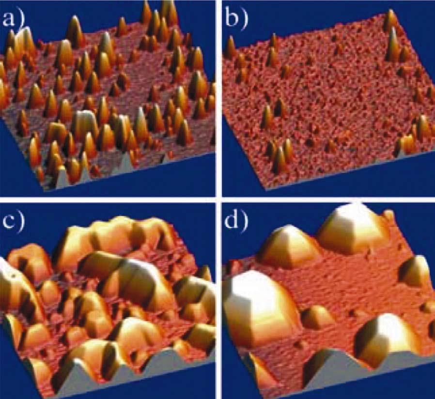
 sample A and b) sample B. The overgrowth of sparse NIs can result in formation of new islands (c). Using increased reactor pressure the formation of new islands during HT overgrowth can be suppressed (d). All the scans are 10 μm × 10 μm.")

A number of important techniques for TD density reduction in GaN templates has already been described in literature. For instance, these techniques include: the introduction of a low temperature nucleation layer before high temperature growth, preliminary substrate nitridation or application of antisurfactant dopants, use of strained interlayers and superlattices, growth of thick buffers, and different variants of the lateral overgrowth technique. For an overview of the existing methods for TD density reduction in GaN layers together with a concise bibliographic list, see Ref. [3]. However, the above mentioned techniques are either not very effective or rather expensive.
The present article describes an effective approach developed to reduce TD density in growing GaN layers by in situ adjusting the growth conditions. Starting point is a physical model which describes the TD density evolution in growing III-nitride layers. Then the experimental evidence of the TD reduction in GaN templates will be provided. Finally, additional technique, which is related to the improvement of template quality by the diminishing of the level of mechanical stresses are discussed, and the role of the advanced approach in the line of other OptoGaN technologies is highlighted.
General Physical Approach
In general, there are three possibilities to control and reduce TD density in growing mismatch layers: to prevent TD generation, to move TDs away from the interior to layer sides (e.g., to the edge of the wafer), and to facilitate reactions among TDs [4]. When considered separately, all the above possibilities can be hardly realized in (0001) grown nitride layers. The nucleation stage is controlled by a high number of nucleation island (NI) sites that is essentially the main reason for experimentally observed high TD density in GaN layers. In principle, lateral dislocation removal can be achieved for patterned substrates (pendeoepitaxy) or during lateral epitaxial overgrowth [5]. However, these methods operate with ex situ sample manipulations and are therefore expensive. TD reactions in (0001) oriented GaN layers have much lower probability than in (001) cubic semiconductor layers. In cubic semiconductors, TDs are inclined. This helps to bring them into reaction distance during layer growth [4,6]. In (0001) nitrides, practically all TDs have their lines parallel to the growth direction and demonstrate no possibility to change mutual distances to react when the layer growth proceeds [7].
This last observation, however, gives a key to the physical basis for a new theoretical approach for TD density reduction in (0001) growth of GaN, which can be described as a two-stage growth of GaN layers. The first stage to facilitate dislocation reactions may proceed via the externally forced dislocation inclination, which can be achieved, for example, by changing to the growth mode of NIs with inclined surface facets, i.e. facets with high crystallographic plane indexes {hk.l}. High index facet plane here means a crystalline plane of wurtzite crystal structure characterized by indexes other than (0001) and those of the type {1-100} and with l ≠ 0 in addition. For this stage I, we designate the layer with intentionally introduced surface roughness as dislocation redirection layer. Then the growth mode should be changed to the preferentially flat (0001) surface to provide enough material volume for dislocation reactions. For this stage II, we designate the growing layer as dislocation reaction layer. The two stages above can be repeated resulting in a multi-stage growth procedure.
Figure 1 illustrates the main ideas of the approach. At the stage of growth before the layer with flat surface is formed, TDs are mostly terminated in the grooves between the neighboring NIs (see dashed lines in figure 1a). In case 3D growth mode is provided during further growth, small neighboring islands are merged into larger islands, and part of vertical TDs is terminated on inclined surfaces of the large islands. For these TDs, it is energetically favorable to change their direction of propagation, provided that the energy barrier preventing inclination of the TDs is overcome (see figure 1a). The inclination of TDs can be facilitated by deposition of a small amount of mask (e.g.amorphous Si3N4) material on the corrugated surface as shown in figure 1b. The TDs will stay at the interface between the new phase and GaN, due to the difference in crystallographic and elastic properties of the deposited material compared to GaN. If subsequent flat surface re-growth by GaN is performed, the TDs will stay inclined and have a high possibility to fuse or annihilate in the reaction layer (see figure 1c). As a result, a compact low dislocation density GaN film may be delivered.
The inclination of TDs in the redirection layer is governed by diminishing the TD energy (because the TD becomes shorter when it deviates to an intentionally introduced high index facet plane) compared with the energy of the TD with line direction along [0001] crystal axis. Additionally, TDs having Burgers vector of the basal plane translation type possess a maximum energy per unit length (described by the energy factor [8]) when their line directions are parallel to the c-axis of the wurtzite elementary cell, i.e. for the case of edge character TDs.
In the dislocation reaction layer, TDs with “frozen-in” inclined directions demonstrate a lateral motion of their intersection points with the planar layer surface (this effect was first explained in Refs. [4,6]). As a result the probability of TD interaction significantly increases, that may lead to the annihilation of two TDs with opposite Burgers vectors or to the fusion of two TDs to produce a single TD. Both these processes provide a decrease of TD density.
Reaction-Kinetics Model for Dislocation Density Reduction
The required thickness of the layers and the number of steps in the procedure depend on the targeted TD density and can be quantatively predicted by applying a reaction-kinetics model to the description of an ensemble of interacting TDs [4]. In accordance with the above outlined ideas, the reduction of the total TD density ρ = ρv + ρi (subdivided into the density ρv of vertical TDs and the density ρi of inclined TDs) should obey the system of the “reaction-kinetic” equations:
Here h is the layer thickness and it plays the role of an evolution variable; the functions on the right hand side, fvredirect , firedirect and fvreact , fireact , describe the processes of vertical TDs redirection, their transformation into inclined TDs and the reactions between various types of TDs. The reaction f-functions depend on a chosen method for substrate manufacturing and therefore include (in a parameterized form) the dependence on growth conditions and the masking process. They also may explicitly include the layer thickness and parameters describing the intensity of TD reactions. We consider an example, for which the reaction functions can be chosen as
For such a parameterization, p is related to the angle α between the facet planes in the redirection layer and the (0001) crystal plane via
p = 1/ γ ⋅ cosα /( 1− cosα) with γ being the coefficient which depends on crystal structure and additional factors (e.g. the presence of a mask material at the grooved surface), κ is the dislocation reaction crosssection parameter. The results for TD density reduction in growing GaN layers for this particular example and with the particular set of model parameters, are given in figure 2. It is important to note that the TD density reduction rate depends on the initial TD density. Higher initial TD density leads to faster TD density reduction. This follows from the fact that at the higher density TDs have an enhanced probability of meeting each other and reacting. Therefore for further TD reduction thicker layers need to be grown, which may restrict the efficiency of this technique, in particular due to the emergence of a high level of mechanical stresses in the template. Nevertheless the clear advantage of the proposed dislocation redirection-reaction approach is that it can be performed in situ by multi-step adjusting of the growth conditions.
Experimental Realization of the Proposed Approach
Growth techniques, which provide efficient TD inclination during the initial stages of growth, become of significant importance for the fabrication of thin GaN layers with lower TD densities. To achieve prolonged high-index facet growth of NIs, a process enabling the reduction of NI density is needed. This would additionally reduce the number of coalescence boundaries between the NIs. We have previously introduced a multi-step MOCVD technique [9] for growing NIs on c-plane sapphire. Here we demonstrate how this technique can help in decreasing TD density in GaN templates.
As a first stage of the multistep method, 3D GaN NIs were grown with a varying number of cycles and with different deposition times per cycle. One process cycle consisted of two steps; the deposition of low temperature (LT) GaN at 530°C and the subsequent annealing of this film for recrystallization as described in Ref. [9]. A TMGa molar flow rate of 60 μmol/min and an ammonia flow of 2 slm were used during the LT deposition steps. The atomic force microscope (AFM) data of figure 3 show the morphology of several samples, in which different methods for NI fabrication were used. The AFM used in our work was a NanoScope IIE system.
Sample A in figure 3a was fabricated with the standard one-cycle method by depositing LT film at 530°C and subsequently up-ramping the temperature linearly to 1060°C in 300 s for recrystallization. The growth process for sample B in figure 3b consisted of four process cycles. The total nominal thickness of deposited material was approximately 50 nm for both samples A and B. Thus, the average thickness of the LT film deposited in each cycle of the multi-step process for sample B was approximately 13 nm. The annealing steps were identical for both samples. The NI density as calculated from the AFM data for the samples A and B was 1×10^8 cm-2 and 2.5×10^7 cm^-2, respectively.
As a second stage of the multistep method, the sparse 3D NIs were overgrown in a way providing a prolonged high-index facet growth for these nucleation centers. The V/III ratio was subsequently increased to 800 in order to promote island coalescence and the resulting dislocation reactions. The increase in V/III ratio additionally stimulates 2D growth and eliminates surface roughening. The NIs were overgrown at high temperature (HT) for 300–700 s in a pressure of 200–500 Torr with a hydrogen flowrate of 10–12 slm. The TMGa molar flow rate was 200 μmol/min and the ammonia flow was 3 slm during the beginning of HT overgrowth to stimulate vertical growth of the NIs. Nucleation in between the NIs was measured by AFM. The GaN island density of about 4×10^7 cm^-2 in figure 3c is higher than the original NI density in figure 3b. For the sample in figure 3c, the reactor pressure and hydrogen flow rate were 200 Torr and 10 slm, respectively. Increasing the total pressure to 500 Torr reduced the nucleation in between the original NIs. This can be observed from the AFM data of figure 3d, where the island density is about 1.7×10^7 cm^-2. The result is caused by enhanced GaN decomposition at a higher pressure [10]. The faster decomposition of the thermally more unstable film in between the NIs suppresses new island formation. This causes nucleation to occur selectively on the original NIs.
Low Dislocation Density GaN Templates
Due to prolonged vertical growth of NIs enabled by a low NI density, more efficient TD inclination is likely to occur. Cross-section transmission electron microscopy (TEM) was used to determine the orientation of TDs inside a NI overgrown at HT with a low V/III ratio. The measured sample was grown in a process which was interrupted prior to the coalescence of NIs. In the TEM data of figure 4 one can clearly observe that an essential part of the TDs incline from the [0001] direction and become perpendicular to a high-index facet of the NI. This type of inclination of TDs inside NIs has not been previously demonstrated by in-situ techniques. The TEM system used in this work was a Philips EM420 electron microscope operating at 100 kV. To resolve for different types of TDs, the diffraction conditions for two mutually perpendicular crystalline planes [0002] and [0110] were fullfilled in cross section and plane view measurements.
See Figure 5 (see LpR magazine)
Several samples were etched in a 1:1 mixture of ortho-phosphoric acid and sulfuric acid after the growth process. The density of etch-pits was subsequently measured by AFM. Figure 5 illustrates the AFM data for two 2.3 μm thick GaN films with etch-pits on their surface. Figure 5a shows the etch-pit density (EPD) for a sample grown by the standard two-step method. A NI density of 1.6×10^8 cm^-2 was used for the nucleation layer. Figure 5b is an EPD scan from a sample grown by the multi-step process. For this sample a NI density of about 5×107 cm-2 was obtained and no surface roughening of the buffer layer was observed. The found EPD was 1.4×10^8 cm^-2 and 5.0×10^7 cm^-2 for the standard sample and for the multi-step sample, respectively. The results of the EPD measurements were also supported by plan-view TEM observations. The experimentally obtained TD density of 5.0×10^7 cm^-2 is in good agreement with the modeling results.
Advanced Technologies for LED Industry
Theoretical and experimental results on the reduction of TD density in III-nitrides and the manufacturing of low dislocation GaN templates give one particular example of the development of advanced technologies for LED industry. Another important aspect in the production of high quality GaN templates and buffer layers is the reduction of the level of internal mechanical stresses in the template interior. A new method for the reduction of mechanical stresses was recently proposed. The method is based on the creation of micro- and nanopores in the semiconductor structures with the help of controlled etching and the following change in the growth regimes of III-nitride layers (see figure 6).
See Figure 6 (see LpR magazine)
The presence of pores in GaN buffer layer allows to enhance the light extraction from LED chips due to effective change of the substrate refraction index. The other technique worked out for efficient light extraction utilizes the insertion of light diffusing interlayer in the chip. Important components of these technologies are directed to the control of physical processes in the working region of the light-emitting heterostructures and to the optimization of the electric current flow in the chip. Both these technologies are covered by national and international patents, e.g. European patent under number EP1903619B1 [11].
Conclusions
We have demonstrated a multistage growth method to substantially decrease the TD density in MOCVD grown GaN epilayers. By reducing the amount of LT material deposited in each cycle of the multi-step process a significant decrease in the NI density was obtained. A low V/III ratio was used to stimulate vertical growth of the NIs before coalescence, which resulted in the formation of large high-index facets for the NIs. This shape of the NIs provides efficient TD inclination during the initial stage of HT growth and subsequently increases the probability of reactions between TDs at the second stage of growth with essentially flattened surface. The proposed method enabled a reduction in the TD density down to 5.0×10^7 cm^-2 and in situ manufacturing high-quality GaN and other III-nitrides templates.
