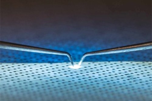
Osram Opto Demonstrates "3D nano LEDs" for White Light and Sees Series Maturity in Coming Years
By making use of nanotechnology, Osram hopes to produce significantly more LED chips with its existing production plant. Osram researchers have for the first time succeeded in manufacturing a so-called "3D nano LED" for white light. The productivity boost is possible due to the special surface characteristics of the LED chip – in contrast to today's standard models, this is not smooth but consists of many adjacent, microscopically small columns with a three-dimensional structure, thus increasing its light-generating area. The new technology is expected to achieve series maturity in coming years, and Osram would then be one of the first companies to use this technology.
The current determining factor for the capacity of an LED chip factory is the wafer size. A wafer has the appearance of a somewhat larger DVD, and functions as a substrate upon which semiconductor materials are applied as thin layers and which is then divided into tens of thousands of single chips. The quantity of chips per wafer is limited by the fact that a specific LED chip surface is required for a certain quantity of light, otherwise efficiency is adversely affected. It's precisely here that the level of innovation with the prototype is to be found. "If you look at the surface of a 3-D nano LED chip under a microscope it looks as if lots of skyscrapers have been built on a flat piece of land," explained Martin Strassburg, Innovation Manager at Opto Semiconductors, a business unit of Osram in Regensburg, Germany. "Put basically, this achieves more façade surface on the same plot of land."
The prototype chip has a five to ten times larger surface on the same substrate than current LED chips, and thereby generates significantly more light in relation to the base area. In addition the luminous efficacy will be increased by approximately 10% in the future. "That would make several thousand additional chips from each wafer, according to the specific model," said Strassburg. To achieve the 3-D chip geometry, a particular masking layer is applied to the wafer above the first deposited semiconductor layers which can be imagined as an ultra-thin glass panel covering the chip itself. Holes are then applied to this with diameters of just a few hundred nanometers, through which the characteristic columns of the Nano LED develop. These columns are then coated with a transparent contact material to ensure that the driving current can spread across the entire surface.
The prototype chip is particularly application-oriented because its surface has already been applied with phosphor material that, as with the vast majority of white LEDs, transforms the initially blue light of an LED into white light. To aid this, a new type of extremely efficient phosphor was developed at the Osram location of Schwabmünchen, Germany, that is especially fine-grained for optimal distribution on the lateral surfaces of the "nano columns".
Following completion of the prototype, the next step consists of reducing colour deviations on thelateral surfaces of the columns to better control the color quality of the spectrum. Industrialization is being simultaneously targeted. "We believe that in coming years we'll be seeing nano LEDs for the first time in large-volume products."
The research of 3D nano LEDs is supported by the ICT FP7 program of the European Union as part of the GECCO project (#280694).


