Plessey Builds LEDs in Cubic GaN on 3C-SiC/Si To Overcome The Green Gap
Plessey, Anvil Semiconductors and the University of Cambridge announced today that they are working together to fabricate high efficiency LEDs in cubic GaN grown on Anvil's 3C-SiC / Si substrates. Cubic GaN has the potential to overcome the problems caused in conventional LEDs by the strong internal electric fields which impair carrier recombination and contribute to efficiency droop. This is particularly true for green LEDs where the internal electric fields are stronger and are believed to cause a rapid reduction in efficiency at green wavelengths known as "the green gap". The availability of cubic GaN from a readily commercialisable process on large diameter silicon wafers is as a key enabler for increasing the efficiency of green LEDs and reducing the cost of LED lighting.
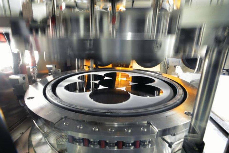
The collaboration, which is partly funded by Innovate UK under the £14m Energy Catalyst Programme, follows on from work by Anvil Semiconductors and the Cambridge Centre for GaN at the University of Cambridge where they successfully grew cubic GaN on 3C-SiC on silicon wafers by MOCVD. The underlying 3C-SiC layers were produced by Anvil using its patented stress relief IP that enables growth of device quality silicon carbide on 100mm diameter silicon wafers. The process is readily migrated onto 150mm diameter wafers and potentially beyond without modification and is therefore suitable for large, industrial-scale applications. Plessey has started to commercialise LEDs produced in conventional (Hexagonal) GaN grown 150mm silicon wafers using IP originally developed at The University of Cambridge. Anvil's high quality 3C-SiC on Silicon technology, which is being developed for SiC power devices, provides an effective substrate, to allow single phase cubic GaN epitaxy growth and provides a process which is compatible with Plessey's GaN on Si device technology.
Keith Strickland, the CTO of Plessey commented: "At Plessey we are constantly striving to find novel technology that can enhance our LED products. The work that has previously been carried out at the University of Cambridge in collaboration with Anvil Semiconductors has demonstrated that high quality cubic-GaN can be grown on large area Si substrates compatible with our manufacturing process. This has opened up the possibility to develop green LEDs with high efficiency that will allow us to demonstrate a new generation of efficient and controllable lighting products."
Professor Sir Colin Humphreys, Director of the Cambridge Centre for GaN, added: "The properties of Cubic GaN have been explored before, but the challenges of growing this thermodynamically unstable crystal structure have limited its development. The high quality of Anvil's cubic SiC on Si substrates and our experience of developing conventional GaN LED structures on large area wafers have enabled a breakthrough in material quality. This latest project will build on our ongoing collaboration with Plessey to deliver, for the first time, green LED devices with efficiency approaching that in blue and red LEDs."
Jill Shaw, CEO of Anvil, added: "Our cubic SiC on Si has unlocked a route to large area growth of cubic GaN. We are delighted to be collaborating on this exciting project that offers the possibility of exploiting our technology in high efficiency LEDs as well as in our core low cost, high efficiency power electronics markets."
Anvil Semiconductors:
Anvil Semiconductors is developing unique silicon carbide power devices. Anvil's alternative approach to SiC switches offers significant improvements in efficiency whilst costing no more than their silicon competitors. This approach involves growing a thin layer of 3 step cubic SiC (3C-SiC) on Si seed wafers sufficient to build the active power devices. In addition to the fundamental crystal growth expertise, Anvil has IP relating to resolving the problem of the stress which is inevitable when growing SiC on Si and which, to date, has prevented this technology from moving forward. The Anvil IP has been proven on 100mm Si wafers and inherently will permit larger wafer diameters to be used without modification. It offers an affordable route to growing high quality cubic SiC which can also be used as a substrate for GaN. For more information see our website www.anvil-semi.co.uk
Cambridge Centre for GaN:
The Cambridge Centre for GaN, a world leading Group, is part of the Department of Materials Science and Metallurgy in the University of Cambridge and is led by Professor Sir Colin Humphreys. It has been actively involved in the development of GaN growth technologies for more than 15 years and is the leading group for GaN materials research in the UK. Through its current activities the Group supplies epitaxial layers to many groups involved in GaN research both in the UK and internationally. It has experience in the growth of GaN layers on to Sapphire, bulk SiC, bulk GaN and large area silicon substrates and in 2011 the intellectual property developed for GaN growth on silicon was acquired by Plessey Semiconductors, who are currently using this technology to manufacture LEDs commercially. The group has a range of EPSRC, EU and industrially funded programmes including a programme grant titled, "Lighting the Future". This is focused on the development of LED structures in GaN and understanding the factors limiting their performance. The group also has projects developing GaN for a diverse range of applications, including electronics, lasers and single photon sources based around its state-of the art MOCVD growth reactors.
Plessey:
Plessey is a leading expert in the manufacture of semiconductor products used in sensing, measurement and controls applications, and is now at the forefront of the Solid State Lighting revolution. Its MaGIC™ (Manufactured on GaN-onSi I/C) LED technology has won numerous awards for its innovation and ability to cut the cost of LED lighting by using standard silicon manufacturing techniques. By using its understanding of electronics and expertise in micro-electronic product design and manufacture, Plessey is radically enhancing the human experience with micro-electronics solutions such that people achieve more than they thought possible. For further information and datasheets, please visit www.plesseysemiconductors.com or email enquiries@plesseysemi.com
