Thermally Activated Degradation of Phosphor-Converted White LEDs
The increasing performances and long lifetime of High Brightness LEDs are still limited by the high temperatures involved. This work shows the results of several accelerated lifetime tests on 1W white LEDs. Two different tests have been carried out: a pure thermal storage at different temperatures and an electrical aging obtained by biasing the LEDs. The impact of high temperatures has been evaluated in terms of flux decay, chromatic properties modification, increase of forward voltage and thermal resistance. A picture of the main degradation mechanisms detected has been provided in detail.
, thermal aged device (center), and the cross section of the electrical aged device, along cathode-anode direction.")


.")
Introduction
Over the last years, the development of Gallium Nitride-based optoelectronic devices covering a wide spectral region from green to ultra-violet has determined a revolution in the lighting industry: thanks to the introduction of high performance device structures (efficacy values above 130 lm/W, [1]), GaN LED technology is targeted to replace the traditional light sources or general lighting, including the light bulbs, with enormous energy savings and environmental benefit.
The environmental advantages of adopting LEDs for general illumination can be easily understood: assuming a 100% market penetration of LED lighting and a 50% conversion efficiency, in the year 2025 the projected electric savings in the U.S. would be roughly 525 TW-h/year (or 35 B$/ year), and the savings in carbon dioxide equivalent emissions would be approximately 87 Mtons.
Furthermore, LED illumination technology eliminates the hazardouswaste issues associated with mercury-containing fluorescent tubes. For this reason, GaN-based LED market is expected to see a rapid growth in the next three years, due to the possibility of adopting these devices for the realization of high-efficiency light sources.
Despite all the improvements that this technology is achieving [2], the main issue of power LED devices is still represented by thermal management. The high junction temperature reached during operation limits the life time of devices and better performing heat sinks are needed in order to operate at high current level. While a few authors reported results for long term stress of AlGaInP LEDs [3], life analysis for normal operating conditions has never been performed on GaN LEDs. Several works reported the impact of high temperature and high current condition on reliability [4-7]. However, a clear picture of the different impact of the current and the temperature on the LED lifetime has never been described.
This paper wants to give a picture of the different degradation mechanisms activated by high temperatures and bias on a family of 1W phosphor-converted LEDs. In particular, several devices have been submitted to an initial characterization in terms of optical, electrical and thermal properties. These properties have been monitored during thermal stress and exhibited a strong degradation. In order to compare results of thermal storage to normal operation condition, an accelerated electrical ageing was performed.
Although the temperatures involved in this work are higher than the maximum ratings specified by the manufacturer, and the devices used belong to an old technology in terms of materials and design, the reader must focus the attention to the importance of adopting smart thermal management solutions in the development of Solid State Lighting applications.
The research activity was carried out in the laboratories of the Microelectronics Group of the University of Padova, Italy. The laboratories are equipped with all the instrumentation of the analysis of the thermal, optical and electrical characteristics of visible LEDs, and for the execution of ageing tests under different bias and environmental conditions. The group has a specific know-how on the analysis of the physical mechanisms that limit the performance and the reliability of electronic devices, and on the definition of models for the explanation of the failure modes and for the extrapolation of the long-term degradation kinetics in electronic devices.
Experimental Setup
The devices used in this work are 1W Phosphor-Coverted white LEDs. The structure of devices is composed of 1 mm^2 area InGaN/GaN LED attached to a copper frame that operates as heat sink. YAG phosphors for yellow conversion are distributed in the protective epoxy that covers the chip. Since the standard deviation of optical and electrical characteristics was below 1% before stress, 5 devices per stress condition have been used in order to have relevant results representative of a larger number of devices.
The main goal of this work is to compare the different degradation mechanisms of devices submitted to pure thermal ageing and dc current ageing. In order to analyze these mechanisms, several characterization techniques have been used. Before ageing the devices, a complete optical characterization has been performed. These measurements were repeated at exponential time steps removing devices from the ageing setup. Furthermore, a thermal analysis was carried out before and after the ageing in order to estimate the junction temperature during stress and the differences in thermal resistance between untreated and aged devices. Light output versus current (L-I) measurements were performed at room temperature by means of an optical power meter equipped with a 2 inch integrating sphere. During the measurements LEDs were biased with a programmable current source able to generate short current pulses, in order to avoid the device self heating. In particular, the devices have been biased and measured with short width pulses (80μs) measurements with a 1s period. Finally, EL spectra were collected by means of a spectroradiometer.
After first selection of devices, parameters for stress conditions were determined. For thermal stress, a climatic chamber at temperatures of 180, 200, 220, and 230°C has been used, with unbiased devices in order to separate degradation mechanisms induced by carrier flow. Although the temperature levels were quite high (the maximal temperature of the junction suggested by the manufacturer is 125°C), the stress conditions chosen could guarantee faster kinetics and, on the other hand, acceleration factors useful to extrapolate life time in nominal operation conditions.
DC current stress has been setup in order to compare the degradation mechanisms generated by different stress conditions. The accelerated stress has been obtained by driving the devices at a current level slightly higher than the nominal one (400 mA instead 350 mA, about 14% above nominal) and without the heat-sink. The evaluation of the junction temperature during stress is very important in order to understand the impact of thermally activated degradation mechanisms. For an accurate estimation of the temperature we used electrical characterization based on forward voltage technique, well described by several authors [9]. The technique consists in a preliminary pulsed mapping of voltage at several temperatures and current levels in order to estimate the parameter. Afterwards the devices were biased at fixed current and once the voltage transient has been collected, the thermal transient has been extrapolated. In figure 1 the thermal transient of one device driven at 400 mA have been reported. As can be noticed, the steady state junction temperature of the device operated at RT was approximately 140°C (115°C+25°C ambient). This fact implies a junction temperature higher than the maximal temperature suggested by the manufacturer, but still lower than temperature level of thermal storage.
Results and Discussion
In the following sections results from both thermal and current ageing have been reported in order to compare the degradation mechanisms owing to different stress conditions.
Light output characterization
Thermal ageing induced a strong optical power lowering, as can be noticed in figure 2, where light output measured at a fixed current of 100 mA (normalized to initial value) has been reported. A nearly exponential decay kinetic has been detected: moreover, the time constant of the degradation process decreased with increasing of the ageing temperature. The plot reported in the figure shows the average of several aged samples: the low values of the error bars confirm that the number of samples used for this work is sufficient for a statistically relevant analysis. In order to clarify the trend of degradation process, we used the time to reach the 70% of light output as the failure parameter (MTTF70%) and we plotted data in figure 3. As can be noticed, the degradation law exhibits an exponential behavior, represented by equation (1):![]()
where k is the Boltzmann constant, T the temperature of storage, and Ea the activation energy of the process that was found to be 1.5}0.1 eV. The extrapolated activation energy was similar to the results of previous works [5]. The developer of the SSL application must be aware that the degradation mechanism found is related to the temperature range between 230°C and 180°C. This means that with Tj<180°C a different activation energy may be found, of course with a lower activation energy. However, the analysis may take a lot of time since the acceleration factor of the stress will be lower.
Similar decay kinetics were detected during accelerated current stress. In figure 4 (see LpR magazine) the average of optical power measured at 100 mA during ageing and normalized to initial value has been reported. The decay induced by current stress was compared to the plot of light output during thermal storage at 220°C. Although the junction temperature during bias ageing was lower than 220°C, the decays were well correlated until 10 hours, implying that the degradation process induced by current ageing cannot be ascribed only to the high temperatures involved during stress. In addition, the plot reports that the light output of devices aged at 400 mA stabilizes after first 10 hours of ageing, while the 220°C aged devices’ efficiency follows the initial exponential decay. For considerations on degradation mechanism acting on lighting decay, further analysis have to be carried out on spectral and package properties, as follows in the next sections.
Spectral analysis
Electroluminescence spectra has been collected before and during thermal stress. In figure 5 one can notice the standard spectrum of Phosphor-Converted white LED, with a blue (InGaN LED) and yellow peak (YAG phosphors). The thermal ageing induced a modification in spectral shape in terms of yellow efficiency. From absolute measurements the lowering of both peaks have been detected.
However the degradation of yellow emission was more enhanced than the blue one and the chromatic yield of device worsened. In order to quantify the spectral modification, the chromatic coordinates X, Y CIE 1931 have been reported in the chromatic diagram in figure 6. As can be noticed, the thermal treatment induced a strong degradation in terms of white yield. In order to understand the level of degradation, the 4–step MacAdam ellipse has been reported for comparison. As widely known, the human eye cannot notice any difference in the colours inside the MacAdam ellipse. This means that after few hours of ageing, a modification of the colour can be noticed. This implies two consequences: (i) after the ageing the colour will not be white anymore and (ii) if two light sources are present in the room and one degrade with higher rate, the colour difference will be detected, and the room will be illuminated by an odd light.
The light output tends to become bluish after ageing and the degradation was observed under all the stress conditions adopted within this work. Considering the ratio between spectral intensity at 560 nm and 456 nm as a degradation parameter, we found that the kinetic followed an exponential decay law, well correlated with the overall light output decay. Thus, the main degradation progress involved in light output decay could be ascribed to yellow conversion of blue light, together with a less predominant lowering of blue emission. This lowering could be ascribed to several mechanisms, i.e. the interaction with hydrogen and the consequent p-dopant passivation, as recently reported in [10]. Concerning the worsening of yellow conversion efficiency, several suggestions on degradation mechanisms could be inferred: (a) the lowering of phosphors efficiency, (b) the browning of the lens, and (c) the degradation of the package [11]. Several authors reported that YAG phosphors employed in LEDs exhibit high stability during operations [4]. The package analysis reported afterwards could provide explanations for the spectral shape modifications.
See Figure 5 (see LpR magazine)
See Figure 6 (see LpR magazine)
Electrical characterization
During thermal and dc current ageing, electrical properties of devices were monitored by means of I-V measurements. The main contribution to the modifications has been detected in the high current range (I > 1 mA) in terms of series resistance increase. The kinetics of voltage measured at a fixed current of 400 mA for representative devices has been reported in figure 7.
See Figure 7 (see LpR magazine)
As can be noticed in the figure, stress induced different kinetics for different stress conditions. Whereas for dc current stress the voltage followed a square root time law, the behaviour for high temperature aged devices was exponential and more enhanced for higher temperatures. Nevertheless, the general trend was very different from exponential decay of light output (figure 4). This uncorrelated behaviour suggest that two different degradation mechanism are responsible for the change in the electrical and optical parameters. For instance, the electrical properties worsening of the contacts in terms of rectifying behavior [12] or detachment from the semiconductor [6]. Since the degradation process that induced the series resistance increase could be ascribed to the structure of the device, a package analysis has been carried out.
Package analysis
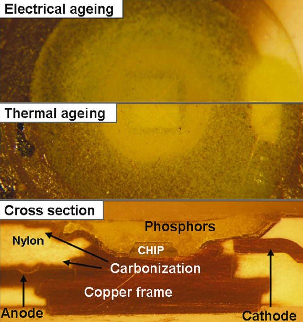
The devices submitted to accelerated life testing showed a visible consequence of the stress in terms of package appearance. After several hours of ageing, the package showed a browning of the white plastic material around the chip. The browning occurred in different patterns. For thermal stress, the package darkened uniformly; on the other hand, the electrical aged devices showed a more enhanced browning at the anode side. In figure 8 the cross sections of aged device has been reported, together with the optical microscope images of the devices submitted to thermal and electrical stress. The different browning pattern detected on the top of the LEDs could be easily understood considering the package design visible in the cross section. The anode is in electrical and thermal contact with the copper frame just below the die attach. This metal mass is the heat sink of the device, and during operating conditions the frame is subjected to high temperature levels. Thus, the plastic around the contact degrades faster than the other side.
The aforementioned worsening of optical properties in terms of light output and spectral properties could be related to the observed carbonization of the package. While the stress affected the white plastic of the package around the copper frame, the reflection properties in the middle remained unchanged. On the other hand, the stress induced a strong decrease in emission in the area around the chip. The light in this region is generated by reflection from side emission of the chip. The browning of the package affected the reflection properties and the lateral blue emission is not enough to excite. To support this hypothesis, the different kinetics of optical power decay in figure 4 could be ascribed to the distinct carbonization pattern in figure 8.
See Figure 8 (see LpR magazine)
The detrimental effects of ageing tests could be ascribed to materials employed for packaging. The materials used for these old generation devices, like the epoxy containing the phosphors or the white nylon composing the package, exhibit a strong sensitivity to high temperature levels. Currently, LED manufacturers are now using more robust materials (like silicon for the lens) and smart package design (phosphors deposited directly on the chip, ceramic package that act as heat carrier and electrical insulator). However, the strong impact of the temperature on the LEDs lifetime must be considered when designing the thermal management of the application.
Thermal analysis
The thermal transients collected before and during ageing could give more information on degradation mechanisms described before. In particular, transients have been elaborated using the structure functions theory in order to extrapolate thermal impedance and other information on the thermal properties of devices. Since the structure of devices analyzed is vertical, we can approximate a uni-dimensional heat flow path from the junction to the copper frame. Thanks to this approximation, the deconvolution of the thermal transient with a weighting function could be performed in order to extrapolate the time constant spectrum. This spectrum represents the lumped-element Foster model for thermal impedance. The Foster model has to be transformed in Cauer network in order to give a physical meaning to the model. Finally, this model can be used to represent the cumulative structure function Cth (heat capacitance per unit length), and the differential structure function K. In particular, this function can we written as
K =ΔCth /ΔRth = cλA^2,
where c is the heat capacitance, λ the heat conductivity and A the cross section area of the heat flow. The two structure functions are plotted using cumulative thermal resistance (K/W) as x-axis [13].
In figure 9 we have plotted the evaluated cumulative and differential structure functions for one representative untreated device and one device aged at 400 mA for 50 hours. From this figure we can extrapolate various information. First, each peak corresponds to a interface or a variation in cross section area along heat-flow path. Thus, the solid line in figure 9 shows two visible peaks at 3.5 K/W and 10 K/W. The first one represents the thermal resistance from junction to chip, while the second is the thermal resistance between junction and the copper frame of the package. The total amount of thermal resistance between junction and ambient is given by vertical asymptote, where the structure function goes to infinite, and is equivalent to 87 K/W (not shown in the figure). This thermal resistance value is so high due to low thermal conductivity of the small copper frame to the ambient. For comparison, we reported in the plot the differential structure functions of aged device. We noticed that the main variations in behaviour were concentrated in the region near the junction, that in the figure corresponds to the region where thermal resistance is below 20 K/W. While the peak corresponding to junction-chip thermal resistance remained almost unchanged for aged device, the peak corresponding to copper case slightly moved towards higher resistance values for aged devices at about 17 K/W. This difference could be related to the worsening of the contact properties during ageing. As reported by [14], stress can induce a partial detachment of contact layer from chip. Contacts play a relevant role in heat dissipation and poor adhesion of metal layer could induce a decrease of thermal conductivity of the device. This hypothesis is in agreement with results on I-V characterization: detachment of contact layer may contribute to series resistance increase.
See Figure 9 (see LpR magazine)
Conclusions
A wide set of white LEDs has been submitted to accelerated life test in order to compare degradation mechanisms and find degradation behaviour and acceleration factors. The life test consisted of high temperature storage and high current biasing. The different stress conditions induced similar degradation mechanism in terms of (a) light output decay, (b) spectral properties modifications, and (c) package epoxy browning. Exponential kinetics of the MTTF70% for thermal aged devices has been detected for high temperature levels. The optical decay could be ascribed to a lowering of blue chip emission and a degradation of yellow conversion efficiency. Concerning blue chip degradation, further work on the bare chip is planned, whereas the worsening of yellow emission has been ascribed to the browning of the package epoxy, suggesting to the manufacturers to use different silicon materials for packaging. Furthermore, an increase of (d) forward voltage, and (e) thermal resistance was detected. The rise in series resistance can be ascribed to chip level degradation, i.e. contact properties worsening or contact detachment. On the other hand, the modifications of thermal properties of the materials (die attach, epoxy) could induce the thermal resistance increase detected for aged devices. The use of silicone materials rather than epoxy plastic for package will improve the lumen maintenance of such devices.
