Yole Développement Announces: Packaging Cost Reduction Is Driving New Technology and Design Adoption
Yole Développement announces today its new report “LED packaging”. Compared to the last edition, this update version provides you an update of all market metrics (packaged LED, equipment, materials…), an highlight of 2012 LED packaging trends (design, new technologies and materials per process step…) and lots of additional analysis (wafer bonding, thermal management at the LED module level…).

Emergence of new design and technologies:
Depending on the device type, packaging can represent 40% to 60% of LED total cost. As such, packaging represents the single-largest opportunity for cost reduction, which is required in order for the industry to access the “Holy Grail” that is General Lighting. However, if you’re expecting this cost reduction to come from standardization, you can abandon all hope. The creativity of LED engineers and specificities of each application have led to an infinite number of package type and formats: Single or multiple chips, low and middle-power Plastic Leaded Chip Carrier (PLCC), ceramic-based high-power LED, small and large arrays, Chip On Board (COB), etc. This profusion of styles is inhibiting LED manufacturing cost reduction by multiplying the Stock Keeping Unit (SKU), thus preventing standardization of the manufacturing process and the associated economies of scale.
In this context, LED manufacturers are reacting by developing new manufacturing philosophies/concepts, such as:
- “Design for manufacturing”, which consists of trying to simplify and standardize elements whenever possible, and push differentiation as far downstream as possible in the manufacturing process.
- “Design for cost”, which consists of favoring cost of ownership or cost per lumen over end-performance.
“Technological developments are also impacted by the quest for cost reduction, and LED manufacturers are now searching for equipment and/or materials with the right mix between cost and performance”, explains Pars Mukish, Technology & Market Analyst, LED at Yole Développement. As a matter of fact, equipment and materials suppliers are proposing more and more equipment and materials that fit these requirements, i.e. laser-based dicer, low-cost ceramic package substrate, etc.
In the end, LEDs are going mainstream but are still not a mature commodity! This is good news for the entire industry, since design and materials innovation still provides opportunity for differentiation. All of this benefits the consumer, who receives budget-friendly, environmentally-friendly and increasingly credible LED-based alternatives for replacing traditional light sources.
Yole Développement’s report represents a comprehensive overview of all technological aspects of LED packaging. It describes each step of the packaging process flow, discusses the associated technological breakthroughs, provides a summary of key players, and much more!
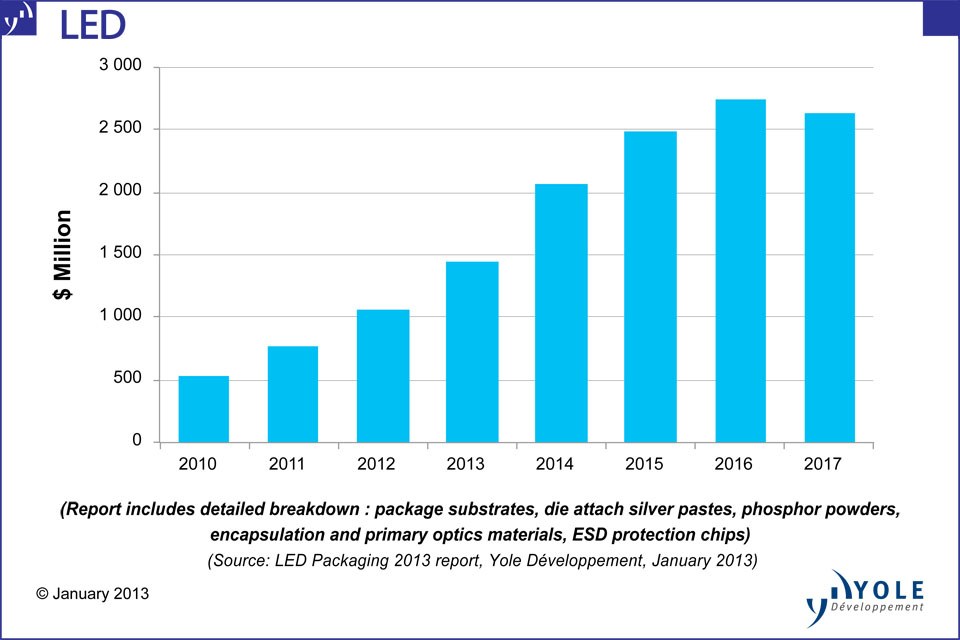
The LED packaging materials market will enjoy a 20% CAGR during the period 2012 - 2017, driven primarily by package substrate and phosphors:
The package substrate market will attain a CAGR of 20% over the aforementioned period, growing to nearly $900M by 2017. Concerning LED phosphors - despite strong price pressure, the associated market will also enjoy double-digit growth, with a CAGR of 20% during the period 2012 - 2017.
In the face of intensifying competition, players are trying to differentiate themselves by proposing an increasing variety of technology options for LED packaging. Substrate material options as well as assembly and interconnection techniques abound as many companies work around the limiting patents of the established players. New players from the general semiconductor markets are proposing new solutions based on their respective capabilities. Similar to IC packaging, new technologies for LED packaging mimic the existing ones, without completely phasing them out -- and there is still a lot of room for innovation, which could lead to more added-value. For such products, however, it remains paramount that the solution offers LED manufacturers an overall reduction in cost of ownership ($/lumen).
At the LED packaging equipment level, growth will return for the next three years:
“The LED packaging equipment market, which stagnated in 2012 due to industry oversupply, is growing again and will peak at nearly $650M by 2016”, announces Pars Mukish
LED packagers are still using mostly retrofitted equipment from the IC industry and relying on existing technology solutions and materials to improve LED cost of ownership and performance. While this has allowed LED manufacturers to benefit from decades of R&D, and investments in the IC industry, it also limits the industry to a space defined by existing technology platforms which are not optimized to the specific needs of LEDs. However, the industry has gained enough momentum in 2011/2012 to entice equipment and material providers into developing dedicated solutions for LED manufacturing.
Many dedicated solutions emerging from both existing and new players will allow significant reduction in LED manufacturing cost through improved yields, throughputs and material efficiency.
The report “LED Packaging” presents all materials and equipment used in LED packaging. It describes market size and volume, trends per process step (performance, price, emerging technologies…), key suppliers, and much more!
- David Jourdan, Yole Développement jourdan@yole.fr
- Faycal El Khamassi, Yole Développement khamassi@yole.fr
For more information about Yole Développement’s technology & market analysis, please click here.
About the “LED Packaging” Report Authors:
Pars MUKISH holds a master degree in Materials Science & Polymers and a master degree in Innovation & Technology Management (EM Lyon – France). He works at Yole Développement as Market and Technology Analyst in the fields of LED, Lighting Technologies, Compound Semiconductors and OLEDs to carry out technical, economic and marketing analysis. Previously, he has worked as Marketing & Techno-Economic Analyst at the CEA (French Research Center).
Dr Eric Virey, holds a Ph-D in Optoelectronics from the National Polytechnic Institute of Grenoble. In the last 12 years, he’s held various R&D, engineering, manufacturing and marketing position with Saint-Gobain Crystals, in charge of Sapphire substrates and materials for optical telecoms. Eric has authored multiple reports for Yole Développement, including Sapphire 2010 and 2011, LED Packaging 2011, Status of the LED Industry, LED Mantech, II-V Epitaxy, and LED Front-End Manufacturing.
About Yole Développement:
Beginning in 1998 with Yole Développement, we have grown to become a group of companies providing market research, technology analysis, strategy consulting, media in addition to finance services. With a solid focus on emerging applications using silicon and/or micro manufacturing, Yole Développement group has expanded to include more than 50 associates worldwide covering MEMS, Microfluidics & Medical, Advanced Packaging, Compound Semiconductors, Power Electronics, LED, and Photovoltaics. The group supports companies, investors and R&D organizations worldwide to help them understand markets and follow technology trends to develop their business. – www.yole.fr
