New Product Enables Higher Quality LED and MEMS Products with Improved Manufacturing Efficiency
KLA-Tencor Corporation (NASDAQ: KLAC), the world’s leading supplier of process control and yield management solutions for the semiconductor and related industries, introduced the next addition to its wafer inspection portfolio, the ICOS WI-2250.
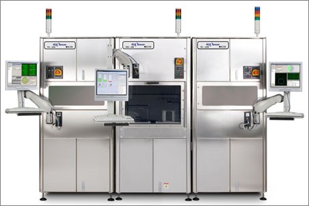

Extending KLA-Tencor’s leading positions within the light-emitting diode (LED) and microelectromechanical systems (MEMS) market segments, the ICOS WI-2250 is a major breakthrough for the industry — offering a dramatic improvement in inspection speed, compared to currently available products, allowing manufacturers to transition to larger LED and MEMS wafer sizes. The ICOS WI-2250 system’s automated optical inspection capabilities enable higher quality LED and MEMS products at increased yields. The new system will allow defect inspection of whole and diced wafers up to 200mm, with macro inspection sensitivity in the pre- and post-dice inspection (i.e., front- and back-end) of high-brightness (HB) LEDs and MEMS wafers.
“The new ICOS WI-2250 addresses our customers’ pre- and post-dice decision needs by helping them overcome the challenge of removing dies that have passed probe, yet still have visible defects, preventing these defective die from entering the expensive packaging process,” said Jeff Donnelly, group vice president, Growth and Emerging Markets (GEM) Group at KLA-Tencor. “In addition, the improved, automated real-time classification and metrology capabilities of the ICOS WI-2250 are designed to reduce operator reclassification and manual metrology measurements, while improving inspection accuracy. That combination will lead to faster cycle time and improved process control, which enables manufacturing efficiency and increased yield.”
Compared with similar products on the market today, the ICOS WI-2250 provides significantly higher inspection sensitivity to critical LED and MEMS process defects. The new system also offers advanced rule-based binning (RBB) for real-time defect classification, advanced metrology capabilities, and faster throughput for inspection as a result of new inspection and data processing technology, which allows an increase in inspection speed. This new solution works in conjunction with the Candela HBLED unpatterned wafer inspection system, to provide comprehensive, yield-improving inspection coverage to the front-end of the line, including analysis for disposition, defect reduction and excursion control.
The ICOS WI-2250 wafer inspection system has received multiple orders. For more information about the ICOS WI-2250, please visit www.kla-tencor.com.
About KLA-Tencor:
KLA-Tencor Corporation (NASDAQ: KLAC), a leading provider of process control and yield management solutions, partners with customers around the world to develop state-of-the-art inspection and metrology technologies. These technologies serve the semiconductor, data storage, compound semiconductor, photovoltaic, and other related nanoelectronics industries. With a portfolio of industry-standard products and a team of world-class engineers and scientists, the company has created superior solutions for its customers for over 30 years. Headquartered in Milpitas, California, KLA-Tencor has dedicated customer operations and service centers around the world. Additional information may be found at www.kla-tencor.com. (KLAC-P).
