OSRAM's New Technology allows for Large Transparent Super Low-Profile OLED
The OLED prototypes that OSRAM Opto Semiconductors has developed as part of a research project are large transparent light sources only a few hundred micrometers thick. Thanks to new technology these organic light emitting diodes do not need separate encapsulation and can be made incredibly thin in any layout.
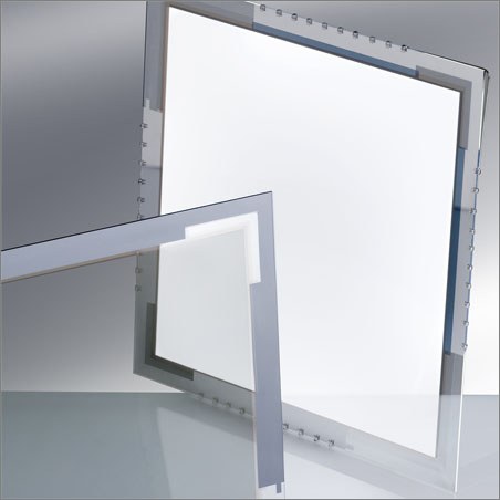

The transparent test samples have a luminous area of 210 cm� and are already showing the enormous potential of OLED light sources. They offer a tantalizing glimpse of the extraordinary lighting applications that may one day become reality.
Even the 17 x 17 cm� OLED panels provide a clear indication of the direction that the OLED lighting market is taking. The demand is for large low-profile transparent light sources. With these samples OSRAM Opto Semiconductors has set an important milestone. The test samples were developed as part of the TOPAS research project funded by the Germany Ministry for Education and Research (BMBF). The aim of the project is to produce 1 m� large transparent OLED modules and will run until 2011.
Even though the modules will have to be made larger they already have many of the properties that distinguish OLEDs from other light sources. They are extremely slim and no longer need expensive encapsulation. Their thickness is now defined only by the substrate as the carrier material � at present this is between 300 and 700 �m. Further development work will lead to an even thinner carrier material and therefore even thinner OLEDs. These low-profile OLED modules will be even easier to use in all kinds of applications. They can be made in any shape, take up very little space and can be integrated so discreetly that they are only noticed when they are switched on. �Transparent OLEDs and flexible OLEDs at a later date will add an entirely new aesthetic dimension to lighting solutions�, said Dr. Karsten Heuser, head of the OLED division at OSRAM Opto Semiconductors. �The possibilities range from light sources that can be integrated in room dividers and furniture, for example, to entire windows that would allow natural light in during the day and flood the room with light at night.� Current OLEDs are being showcased at PLDC (Professional Lighting Design Convention) from October 29 to 31, 2009 in Berlin to demonstrate the latest state of development. The panels provide an impressive foretaste of future applications in which designers can let their imaginations run wild.
The OLED panels can be made transparent without any detracting structures. This is thanks to new developments in electrode design, a special component architecture and a new approach to thin-film technology. Without any additional conductor path structures on the light-emitting surface, the current is distributed evenly over the active surface, which in turn leads to uniform luminance. The new technology also simplifies the manufacturing process, whether OLEDs are produced on a small molecule or polymer basis. Irrespective of the material of the active layers, the technology can be used for colored, warm white and cold while OLEDs. The next stage is to integrate the processes into a stable manufacturing operation.
OSRAM is part of the Industry sector of Siemens and one of the two leading lighting manufacturers in the world. Its subsidiary, OSRAM Opto Semiconductors GmbH in Regensburg (Germany), offers its customers solutions based on semiconductor technology for lighting, sensor and visualization applications. OSRAM Opto Semiconductors has production sites in Regensburg (Germany) and Penang (Malaysia). Its headquarters for North America is in Santa Clara (USA), and for Asia in Hong Kong. OSRAM Opto Semiconductors also has sales offices throughout the world. In the 2007 fiscal year (to the end of September) OSRAM Opto Semiconductors employed more than 4000 people and achieved sales totaling 520 million euros.
