A Study on Aerosol Jet Printing in LED Module Manufacturing
LpR 68 Article, page 38: LED module manufacturing technologies have certainly improved over the last few years but the requirements have also increased. More components are packed on today’s modules causing additional thermal stress, and, at the same time, the demand for lower cost challenges module manufacturers. So the (re-) search for new materials and new manufacturing processes and manufacturing technologies is still on. Paul Hartmann, Director of the Institute of Surface Technologies and Photonics at the Joanneum Research Forschungsgesellschaft m.b.H., and his team, Andreas Rudorfer, Martin Tscherner, Christian Palfinger, Frank Reil, Franz P. Wenzl with Ioannis E. Seferis, Eugeniusz Zych from the Faculty of Chemistry of the University of Wroclaw investigated the opportunities of aerosol jet printing and proved the applicability for alternative ways of phosphor deposition and integration and to replace wire bonding of dies.
Abstract
Modern LED packaging technologies have to satisfy the demand for integrating an ever increasing number of components into a module to achieve high light intensity, dynamic color temperatureand light intensity control and high product reliability, while targeting low production costs. State-of-the-art LED dice packaging based on Chip-on- Board (CoB) technology comprises some shortcomings both of the manufacturing process and tolerances but also with regard to potential sources of failures. The extreme thermal conditions LEDs experience in particular in general lighting applications lead to heavy stress of the bonded wires exerted by surrounding silicone due to different thermal expansion coefficients.
Therefore, there is a clear need for alternative packaging processes. A promising technology in this regard is additive manufacturing. While ink-jet printing has gained some attention during the last years due to its material and cost saving potential, aerosol-jet printing has recently demonstrated many advantages. With the latter technology it is possible to print highly viscous inks containing particles up to a diameter of 1 μm and to deposit more material during a single printing step. Based on these technological advantages circuits with a higher ampacity can be realized.
Based on test samples and test structures, in this contribution the potential of aerosol-jet printing in various aspects of LED module packaging will be discussed, ranging from the deposition of the die-attach material, wire bond replacement by printed electrical interconnects to aspects and new concepts for phosphor deposition and integration.
Introduction
Light-emitting diodes (LEDs) are currently conquering the market for general lighting [1, 2]. However, there are still many challenges ahead before LED based luminaires will realize their full potential in terms of energy efficiency and white light quality [3]. Besides these quality features, which are directly related to comfort and well-being, also the reliability of the luminaires is of particular relevance for convincing people to abandon traditional lighting sources and to replace them by those based on LED technology.
With respect to reliability, state of the art fabrication of LED modules based on chip-on-board (COB) technology comprises some shortcomings both with respect to the manufacturing process itself but also with regard to potential sources of failures and manufacturing impreciseness. For instance, the electrical contacting of LED chips with surface-mounted contact pads is based on wire bonding, with the wire bonds encapsulated in a silicone layer for mechanical protection. For white light generation, phosphor particles are added to this silicone layer, forming the so-called color conversion element (CCE). The extreme thermal conditions LEDs experience in particular in general lighting applications, lead to heavy stress between the bonded wires [4, 5] and the surrounding silicone, because of their different thermal expansion coefficients. In particular, despite the overall thermal load, one also needs to consider the differences in temperature, which may occur within this silicone layer.
As a result of the low thermal conductivity of silicone and the heat induced in the phosphor particles upon the color conversion process (Stokes shift, quantum efficiency lower than unity), the highest module temperatures are often located inside the CCE, in particular nearby its top surface. Depending on parameters like the drive current, the quantum efficiency of the phosphor and the thermal conductivity of the matrix material, the temperature differences between the bottom part and the top part of the CCE may reach values in the range of more than 100 K [6]. As a result, the wires may break, resulting in an imminent failure of the module.
Also state of the art manufacturing technologies for the CCE itself comprise some shortcomings with regard to the fabrication of CCE architectures that support superior white light quality and good heat dissipation. For example, dispensing, the most common method for phosphor deposition, suffers from low accuracy. In addition, wire bonds may also negatively affect the geometry of a CCE [7].
Therefore, there is a clear need for alternative fabrication processes. A promising technology in this regard, which offers the potential for a more proper system configuration and integration in many aspects of module manufacturing, is additive manufacturing, a technology which has gained a lot of attention during the last years due to its materials and cost saving capabilities.
Additive printing technologies caused a paradigm shift in various technological sectors [8]. An increasing demand for new innovative, functionalized materials and corresponding process technologies, especially in the field of printed electronics, currently gives rise to an enormous number of academic and industrial research activities. Additive manufacturing is also suitable for direct fabrication of electrical interconnects on nearly any rigid and flexible substrate. According to market research companies such as IdTechEx this market will grow dramatically within the next 10 to 15 years.
For some time conductive and insulating structures on various substrates were mostly fabricated by ink jet printing. First attempts of fabricating LED modules by electrical interconnects made by ink jet printing have already been reported [9, 10]. But the use of ink jet printing is limited due to the need for high currents and low resistivity of electrical interconnects in LED operation. Other disadvantages of ink jet printing are: low viscosity of the ink, low solid contents and a limited particle size due to the nozzles geometry as well as the need for a low standoff distance to the substrate. Therefore, a mounted die may obstruct the nozzle, which runs counter to the demand for integrating an ever increasing number of components (photo diodes, sensors, etc.) into a module to comply with the customers’ expectations, such as high light intensity, dynamical color temperature- and light intensity control, and so forth.
In comparison with ink jet printing, aerosol jet printing has demonstrated many advantages when printing high precision electronic circuits on 3D substrates. Using aerosol jet printing it is possible to print highly viscous inks containing particles up to a diameter of 1 μm and to deposit more material during a printing step. Based on these technological advantages circuits with a higher ampacity can be realized. A higher ampacity is an essential requirement for a better device performance. Due to the fact that aerosol jet printing allows for a much larger distance between the nozzle and the substrate surface, it is also possible to manufacture modules with a much higher dice integration density.
In order to exploit these advantages, the applicability of aerosol jet printing is investigated in many fields of application. Several scientific publications discuss the use of aerosol jet printing for organic solar cells [11], thin film transistors [12], the fabrication of ring oscillators [13] or the development of novel fuel cells [14]. Nonetheless, with the exception of some patent applications, publications dealing with the application of aerosol jet printing for the fabrication of LED modules are rare.
In the following, we address some of the challenges with respect to the module fabrication outlined above and discuss the potentials of aerosol jet printing in this regard. Within this work, the die-attach material, the electrical interconnects to the LED dice and the phosphor materials are applied by aerosol jet printing in order to fabricate a white light emitting LED module.
Experimental Methods
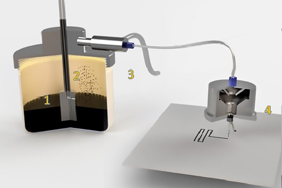
For aerosol jet printing (Figure 1 - scheme of the process), the ink is placed into a pneumatic or ultrasonic atomizer that creates a dense aerosol of droplets (1) with diameters ranging from 1-5 microns (2). The aerosol jet printing process with the pneumatic atomizer is influenced by a number of (adjustable) parameters, including ink temperature, carrier gas flow rate, exhaust gas flow rate sheath gas flow rate, nozzle diameter, tube heater temperature, working distance, stage speed, and stage temperature. Subsequently the generated aerosol is carried by a gas (N2) flow to the deposition head (3). Within the deposition head (4) the aerosol is focused by a second gas flow (sheath gas). The resulting, high velocity converging particle stream is deposited onto the substrate creating fine features with line widths down to 10 μm. The line shapes and/or the written patterns can be designed using CAD. During the deposition process there is no physical contact between the material being printed and the nozzle. This allows keeping the critical areas of the print system clean and free of material build up preventing nozzle clogging and particle stream interruption.
 Figure 1: The heat load is Principle of Aerosol jet® printing
The process has a natural standoff distance of 1- 5 mm or more between the nozzle and the substrate. Therefore conformal writing on 2D or 3D surfaces can be performed without changing the z-position of the nozzle within a range of a few millimeters.
In this study, the following printing system and materials were employed. For aerosol jet printing an Aerosol jet 300CE Deposition System from Optomec Inc. was used. For the die-attach material a silver nanoparticle filled epoxy, ACURA E8074 from Resin Designs LLC, designed for dispensing through an Optomec Aerosol jet system was used. For the isolation layer a polyimide (Sigma Aldrich) diluted with n-Methyl-2-pyrrolidon (NMP), ratio 1:2, was the material of choice and the electrical interconnects were fabricated from a conductive ink based on silver nanoparticles for aerosol jet printing, PG-007 from PARU. For the phosphors either a Yttrium aluminium garnet activated by cerium (Ce:YAG, with the phosphor particles milled in-house with a ball mill to smaller, printable particle sizes of 1 μm and below as will be discussed elsewhere in detail) or a fine powder of Lutetium aluminium garnet activated by cerium (Ce:LuAG) [15] was used. Besides the Ce:LuAG phosphor, the related ink was fabricated from Disperbyk D-142, AZ125-NXT, PGMEA and Veratrol. The LED-dice used are dice in vertical thin film configuration (with one contact on the top and the other at the bottom of the die). In particular, Cree EZ 500 Gen II and Cree EZ 900 Gen II (in case of printing the “LED” symbol on top of the die) dice were used.
 Figure 2: Schematic of replacing the wire bond for contacting the top contact pad of an LED module by printed electrical interconnects. Firstly an insulation layer is printed on top of the bottom contact pad and the sidewalls of the LED die, subsequently an electrically conductive material is printed on the top of the insulation layer to form the electrical interconnect. To electrically interconnect the bottom contact pad and the LED die an electrically conductive die-attach material is used, which is also deposited by Aerosol jet printing
Figure 2 shows a schematic of an LED die mounted on a printed circuit board (PCB) for which the wire bond (left side) for connecting the top contact is replaced by a printed interconnect (right side). For electrical insulation in case of the printed interconnect, first an insulation layer (covering the bottom contact pad and the sidewalls of the LED die) is printed and the electrically conductive interconnect is printed on top of it. In this work the print head was mounted in a 45° angle using a special tilt fixture.
Generally, printing over chip sidewalls and contact pads requires either tilting of the substrate or the print head in order to achieve sufficient surface coverage. In addition, due to shadowing effects it is not always possible to print the whole interconnect from the same position of the print head. For instance, as shown in figure 3, from printing position 1 it is possible to print the isolation layer and the electrical interconnect on the sidewalls of the die as well as on the bottom contact pad, however, some parts of the top contact pad are shadowed for printing position 1. Therefore, for printing the whole electrical interconnect (connection to the top contact pad) the nozzle arrangement (printing position 2) was changed (Figure 3).
 Figure 3: Printing scheme: On the bottom contact pad and on the sidewall of the LED die the insulation layer and the electrical interconnect on top of it are printed from printing position 1. Since for this configuration some parts of the top contact pad are shadowed, the printing head is brought into printing position 2, from which the electrical interconnect on the top contact pad is printed
Results and Discussion
Die-attach material
As a first step in the fabrication process of a white light emitting LED module the die-attach material is printed onto the bottom contact pad. Using aerosol jet printing, the required amount of material can be precisely controlled and tuned e.g., to the chip size. Too little or too much of the die-attach materials might lead to either an open contact between the die and the contact pad (which also impedes heat transfer) or a short circuit in case the die-attach material climbs up the sidewalls of the die. To demonstrate the flexibility of materials deposition, in the left image of figure 4 both a contact pad and an electrical interconnect were printed from the die-attach material on a glass substrate. Subsequently, a chip was mounted by applying an appropriate amount of die-attach material. This process is used in the following to deposit the die-attach material on the bottom contact pad of the PCB.
 Figures 4: Printed contact pad and interconnect, both printed from the dieattach material on a glass substrate (left). Subsequently, an LED die is placed on the die-attach material (right)
Electrical interconnect
In the first step of the electrical interconnect formation procedure a polyimide layer was deposited on a sidewall of the LED die and on the bottom contact pad serving as an insulator as well as a smoothing layer (for the electrical interconnect layer). The thickness of the insulation layer can be tuned by printing several layers on top of each other. Albeit thicker layers are in advantage to lower the risk of short circuits, they might pose the problem of (micro) cracks during curing. Therefore, the height of the insulation layer was selected in the lower 10 μm range.
 Figure 5: Profilometer scan of the electrical interconnect on the polyimide layer
Subsequently, PG-007 was printed onto the insulation layer to form an electrical interconnect with a width of 40 μm and a height of about 30 μm. Figure 5 shows the profile of the electrical interconnect on the polyimide layer as determined with a profilometer, figure 6 images of the resulting LED module under operation.
 the LED die under operation (right)") Figures 6: LED module with a blue emitting LED die (left) the LED die under operation (right). Both the die-attach material and the electrical interconnect were deposited by Aerosol jet printing
Figures 6: LED module with a blue emitting LED die (left) the LED die under operation (right). Both the die-attach material and the electrical interconnect were deposited by Aerosol jet printing
 Figure 7: Onset behavior of the I/U characteristics of 13 LED modules with the die-attach material and the electrical interconnects deposited by Aerosol jet printing. The onset behavior is in good accordance with the data sheet
Phosphor deposition
In the final step of the fabrication of a white light emitting LED module, the phosphor layer is printed on top of the LED die. Figure 8 shows an LED module, on which in addition to the fabrication steps shown in figure 5 also the phosphor layer (Ce:YAG) was deposited by aerosol jet printing.
 Figures 8: LED with the printed die-attach, printed electrical interconnects and a printed phosphor layer on the top of it in the off-state (bottom left) and under lowcurrent operation (top and bottom right). The phosphor is a conventional Ce:YAG phosphor that was milled with a ball mill down to particles sizes of 1 μm and below
It is still more convenient for aerosol jet applications to use phosphors synthesized with small particle sizes than to mill down conventional 10 μm phosphors. Therefore, in particular nano-sized phosphors are very promising for aerosol jet printing of a phosphor layer. In order to highlight the achievable preciseness, experiments were also performed with a Ce:LuAG phosphor with particle sizes in the nanometer range. Figure 9 shows an optical microscope image of a printed square (4 printed layers one above the other) from such a phosphor on a glass substrate as well as a fluorescence microscope.
 and fluorescence (right) microscope images of a square printed from the nanosized Ce:LuAG phosphor") Figures 9: Optical (left) and fluorescence (right) microscope images of a square printed from the nanosized Ce:LuAG phosphor
Figures 9: Optical (left) and fluorescence (right) microscope images of a square printed from the nanosized Ce:LuAG phosphor
Still, in order to demonstrate the high precision in the deposition of the phosphor layer that can be achieved by aerosol jet printing, a “LED symbol” was printed (5 layers) on a glass substrate using the Ce:LuAG phosphor. Figure 10 shows a fluorescence microscope image of this LED symbol on the glass substrate as well as an optical microscope image of an LED under operation on which the same LED symbol was printed (Cree EZ 900, Gen II with conventional electrical interconnects by wire bonding). The precision and the flexibility of aerosol jet printing for CCE deposition and shaping are therefore clear advantages, considering the importance of the geometry of a CCE and its exactness with respect to the white light quality of an LED [17] as well as the need for some specific shapes (e.g., with respect to efficacy, alternating areas of two phosphors in horizontal direction are preferable in comparison with two phosphor layers on top of each other [18]).
 Figures 10: Fluorescence microscope image of an LED symbol printed from the Ce:LuAG phosphor on a glass substrate(left). LED with an LED symbol printed from the Ce:LuAG phosphor on top of it under operation (right)
Conclusions
Additive manufacturing using aerosol jet printing technology was shown to offer a great potential as an alternative technology for the deposition of the die-attach material and the electrical interconnects of an LED module, for nowadays at least in low power devices. In addition, high precision deposition of the phosphor layers for color conversion was demonstrated, which can be employed even in high power applications.
Acknowledgements:
Financial support from the Austrian bmvit, Project AeroPack, is gratefully acknowledged. The authors also thank C. Auer for performing the profilometer measurements and Tridonic Jennersdorf GmbH for providing the PCBs.
References:
[1] M. R. Krames, O. B. Shchekin, R. Mueller-Mach, G. O. Mueller, L. Zhou,
G. Harbers, M. G. Craford, J. Display Technol. 3, 160 - 175, (2007)
[2] J. Y. Tsao, M. H. Crawford, M. E. Coltrin, A. J. Fischer, D. D. Koleske,
G. S. Subramania, G. T. Wang, J. J. Wierer,R. F. Karlicek,
Adv. Optical Mater. 2, 809 - 836, (2014)
[3] J. Brodrick, http://apps1.eere.energy.gov/buildings/publications/pdfs/ssl/feb2013_nema_brod
[4] Z. Chen, Q. Zhang, R. Chen, F. Jiao, M. Chen, X. Luo, S. Liu,
Proc. of the Electr. Comp. and Technol. Conf. 2011, 454 - 459
[5] Z. Chen, Q. Zhang, F. Jiao, R. Chen, K. Wang, M. Chen, S. Liu,
IEEE Trans. Compon. Packag. Manuf. Technol. 2, 1135 - 1142, (2012)
[6] P. Fulmek, C. Sommer, P. Hartmann, P. Pachler, H. Hoschopf,
G. Langer, J. Nicolics, F. P. Wenzl, Adv. Optical Mater. 1, (2013),
753 (2013)
[7] B. Wu, X. Luo, H. Zheng, S. Liu, Opt. Express 19, 24115 - 24121, (2011)
[8] S. Mellor, L. Hao, D. Zhang, Int. J. Prod. Econ. 149(2014) 194-201
[9] W. Shen, X. Zhang, Q. Huang, Q. Xu, W. Song, Nanoscale,
6(2014) 1622-1628
[10] M. Wu, Z. Gong, D. Massoubre, Y. Zhang, E. Richardson, E. Gu,
M. D. Dawson, Appl. Phys A 104, 1003-1009, (2011)
[11] P. Kopola, B. Zimmermann, A. Filipovic, H.-F. Schleiermacher,
J. Greulich, S. Rousu, J. Hast, R. Myllyl, U. Würfel; Sol. Energ.
Mat. Sol. Cells 107, 252-258, (2012)
[12] Se Hyun Kim, Kihyon Hong, Keun Hyung Lee, and C. Daniel Frisbie;
ACS Appl. Mater. Interfaces 5, 6580−6585, (2013)
[13] M. Ha, J.-W. T. Seo, P. L. Prabhumirashi, W. Zhang, M. L. Geier,
M. J. Renn, C. H. Kim, M. C. Hersam, C. D. Frisbie; Nano Lett. 13,
954-960, (2013)
[14] M. Sukeshini A., F. Meisenkothen, P. Gardner, T. L. Reitz;
J. Power Sources 224, 295-303, (2013)
[15] I. E. Seferis, E. Zych, J. Lumin. 169, 838 - 843, (2016)
[16] www.cree.com
[17] C. Sommer, F.P. Wenzl, J. R. Krenn, P. Hartmann, P. Pachler,
M. Schweighart, S. Tasch, G. Leising, Opt. Mater. 31, 837 - 848, (2009)
[18] S.-P. Ying, J.-Y. Shen, Opt. Lett. 41, 1989-1992, (2016)
