Automatic Panel Level Transient Thermal Tester
LpR 67 Article, page 44:The thermal resistance junction in case is an important parameter for the reliability of LEDs because degradation of the LED is temperature driven. Simulation and testing has advanced over the past few years but transient thermal analysis (TTA), which is required to understand the thermal transfer path, is especially work and time consuming - and not automated. Gordon Elger, Professor for Electronic Manufacturing Technologies, Technische Hochschule Ingolstadt, and his co-authors, Maximilian Schmidt, Alexander Hans, and Dominik Müller, present and discuss an automatic panel level TTA tester. They explain the challenges and the solution and demonstrate the applicability of using LED test board-panels.
Introduction
Today, LED systems can be differentiated not only by high power, mid power and low power application, but also concerning reliability, i.e. high reliability and low reliability. On the one side, low cost LED consumer goods and, unfortunately, partly also replacement LED bulbs are located at the low reliability side of the lighting applications. On the other side, reliability and long lifetime determines the economic and ecological success of high-end LED illumination systems, e.g. outdoor illumination, signaling, agricultural LED systems and automotive lighting. LED lighting systems can, in general, reach very long lifetime of up to 100,000 h when appropriate designed and business models are based on the failure free operation of the light sources. Junction temperature and drive current are the key parameters that determine lumen degradation. In addition to the slow lumen degradation also catastrophic failures of the LED can occur. For eliminating these failures not only die and package design but also process and material control in manufacturing is important. Finally, the environmental conditions during operation like humidity, corrosive atmosphere and thermo- mechanical stress are fundamental for the lifetime of the LED systems.
Because many failures are driven by the junction temperature TJ of an LED, thermal management is essential to realize cost competitive but reliable LED systems. Transient thermal analysis (TTA) is a powerful approach to measure the junction temperature of the LEDs in a system and the thermal resistance Rth_el of the LED module [2-4]. A method for the automation of this process will be demonstrated in this paper.
How Transient Thermal Analysis Works
After switching a heat load, i.e. switching the LED drive current from high heating current to low sense current, the forward voltage Vf(t) is measured time resolved. The thermal path from the die through the LED package to the heat sink can be resolved. TTA has become a common method and it is standardized in the MIL-STD-750F (3100 Series) [5]. Also the Solid State Technology Association (JEDEC) published valuable standards and thermal characterization test methods [6] in their JESD51 series. They are applicable to a wide variety of semiconductor packages under different mountings and usages conditions and underpin the thermal specifications of the manufacturer. TTA can also be applied for reliability testing. The location of failures can be identified. For example, it is possible to distinguish between failures such as delamination of the LED die or cracking of solder interconnect from the LED package to the printed circuit board (PCB) [7]. However, the TTA measurements are often considered as complicated and time consuming. The thermal load which is switched, i.e. the electrical energy minus the optical energy, and the proportional factor between temperature and forward voltage have to be measured to calculate the real thermal resistance Rth_real (Symbols used as defined in JEDEC51-51: Rth_el: electrical-thermal resistance using as thermal load the electrical power, Rth_real: real thermal resistance using the real thermal load). To reduce the measurement effort, the relative thermal resistance method was introduced [1]. By relative thermal resistance measurement the k-factor and thermal load are not measured, but obtained by thermal path normalization to reference samples, i.e. known good samples, for which thermal load and the k-factor are known, i.e. precisely measured. To obtain the Rth the thermal response need to be measured as early as possible after switching the heat load, in especially to resolve the thermal resistance between die and first heat spreader or substrate (first level interconnect). The measurement dead time and resolution depends on the electrical response of the equipment and the sample itself, i.e. parasitic capacity of the LED and parasitic inductance of the equipment. Typical well-designed and maintained equipment reaches 20μs dead time. Signal cable length and electromagnetic noise influence the switching time and the stabilization of the detection current and therefore the measurement signal. Often every individual set-up in a lab, even from the same supplier, can behave differently. The errors influence the data evaluation and results. Especially in the structure-function, the dominating approach to analyze the transient temperature data, is influenced by the dead time and the method how to extrapolate the very early Vf(t) data. It plots the cumulative thermal capacitance Cth in dependence of the cumulative thermal resistance Rth alongside the heat flow path (one dimensional approximation). Most of the artifacts which influence the structure function are visible in the time domain, i.e. visible in the time derived Vf(t) curve and could be detected before further data processing.
Today, TTA equipment migrates from lab equipment to automatic inline inspection for quality control and reliability analysis. However, high time resolution and dead time to access the first level die contact is not yet commercially available as an automatic in-line tester. In this paper an automatic panel level LED tester with the focus on reliability testing of LED on wafer or panel level is presented. The performance of the electronic hardware, the automation approach, the automatic data evaluation and test report generation is developed and described.
Transient Thermal Analysis
Method based on JEDEC 51-14 and JEDEC 51-51
To determine the Rth junction to case, the temperature gradient within a LED system has to be measured. The forward voltage Vf of the junction can be used as a temperature probe due to its quasi linear temperature dependence. Actually, the dependence is non-linear and can be derived from semiconductor theory by the Shockley equation. However, in an adequate small temperature range (within 30-50°C) it can be linearly approximated for a defined drive current(EQ1).
Approximation of Vf for a limited temperature range:
 EQ1
EQ1
The constant factor k, called the k-factor (sensitivity s=1/k) defines the relation of Vf(t) from temperature T. The sensitivity s is in the range of 2 mV. The constant Ucon is due to contact resistance of the probing system and the inner serial resistance of the LED. The k-factor depends on the energy bands and the effective electronic state densities of the junction and, therefore, also from internal and packaging induced stress in the junction. The sensitivity s may vary for a single LED from wafer to wafer batch between 1 mV and 3 mV. After determination of the k-factor for a specific drive current, the forward voltage can be used to calculate the temperature change in the LED junction when the specific current is applied. However, the k-factor can change during reliability testing in dependence of the device and epitaxial design of modern LEDs. The same holds for the LED efficiency. The lumen flux as well as the thermal load, change during accelerated testing of the LEDs. Therefore, to obtain the accurate thermal resistance Rth_real the k-factor and the lumen flux need to be measured again after every interval of accelerated lifetime testing. This causes a significant amount of experimental effort and is not adequate for large volume reliability testing or in-line inspection.
 Figure 1: The heat load is switched using the drive current of the LED. During heating up under high drive current Vf decreases from the initial large value because the junction heats up. Due to switching from large heating to small sensing current Vf is initially reduced because the required Vf at lower current is smaller (V(I) characteristic curve) and rises afterwards while the junction cools down
As discussed in the introduction, the transient thermal analysis is a common method to measure the thermal resistance of microelectronic packages that contain active semiconductor devices. The thermal response of a system like an LED package on a printed circuit board is measured time resolved after switching a heat load as shown in figure 1. Initially a constant heat flux is applied by a large drive current (Iheat) until the thermal equilibrium is reached. The thermal equilibrium is then changed by switching off the heat flux. The forward voltage Vf(t) is measured time resolved applying a small sensing current ISense while the system transfers into its new thermal equilibrium. The temperature T(t) is obtained from Vf(t) by equation (1). For accurate absolute temperature measurements Ucon, i.e. the contact resistance, in equation (1) needs to be small or very reproducible. Transient testing determines the difference ΔVf = Vf (junction hot) - Vf (junction cold) and is independent from Ucon and by that independent from the contact resistance. However, one needs to measure the Vf for hot condition, i.e. heat flux switched on for a sufficiently long time so that the thermal equilibrium is reached, and Vf for cold condition (heat flux switched off for a sufficiently long time so that the thermal equilibrium is reached) for the same drive current ISense. After switching off the drive current from IHeat to ISense a delay time, i.e. dead time, is required until the system has stabilized after current switching before accurate Vf data can be obtained. The dead time is discussed in more detail in section 3, below. The same holds rue when measuring the heating up of the device and besides that, under high current conditions noise is increased. In addition, while heating up the thermal load changes due to change of WPE in dependence of the temperature. Cooling down measurements are therefore preferred. However, for in-line measurements also heating up data are useful and utilized.
Based on the transient Vf(t) measurement the transient thermal impedance Zth(t) is calculated:
 EQ2
EQ2
Following the Jedec51-14 (Apendix B), the logarithmic time derivation of Zth(t) is calculated. First the time is substituted by the logarithmic time z=ln(t):
![]() EQ3
EQ3
Afterwards the logarithmic time derivation is obtained:
 EQ4
EQ4
The approach for dead time correction is described in JEDEC51-14 in section 4.3 (Offset correction). The widely spread approach is the square root correction. However, the time interval for which the square root correction is performed is not generally defined in the standard. From a practical point of view the shortest possible time interval is used. However, it depends on the dead time of the experimental equipment. In most papers published on TTA, the dead time correction is not described appropriately. To compare TTA measurement performed with different equipment the square root correction intervals have to be defined equally. The structure function is obtained after the calculation of the time constant spectrum R(z) for the Foster-Representation and afterward by Foster-Cauer transformation. However, in this paper the structure-function is not used for automatic TTA analysis. Automatic TTA analysis is based on the transient time data to filter out measurement errors that are better visible on the time domain. The relative thermal resistance method utilizes solely the b(z) curve for thermal path analysis. Later on, the structure function can be calculated in addition.
Relative Rth Measurement
As discussed in the previous section, for determination of the real thermal resistance Rth_real in addition to the transient Vf(t) curve, the k-factor and the thermal load have to be measured. The relative thermal resistance method avoids this by relative measurement. Using calibrated known good samples the Rth_real is calculated. In the following, the concept of the relative thermal resistance measurement for reliability testing will be explained.
The concept is rather straight forward and nothing more than a normalization after the logarithm of b(z) is calculated:
 EQ5
EQ5
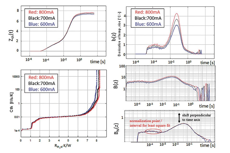
The effect of the logarithm is straightforward. Linear factors are transferred to an axis offset. The efficiency of the method is depicted in figure 2. When measuring an LED at different current slight changes in the efficiency changes the Zth(t) curve. This is also visible in the b(z) curve and the structure function. However, in the B(z) curve it can be noticed that the heat path doesn’t change: all B(z) curves are solely moved perpendicular to the time axis. In the following, normalization will be called the process “moving the B(z) curves perpendicular to the time axis” to match the B(z) curve on a known good sample. After normalization the index N is added, i.e. BN(z) are the normalized B(z) curves. The normalization is performed by a least square root fit of an axis offset.  Figure 2: General description of the relative Rth method. - The heating current is varied in the measurement. The dead time in this example is 20 μs. Time data before 20 μs are eliminated, i.e. the square root extrapolation is not used. The optical efficiency changes with the heating current, therefore the Rthe_el changes. The optical efficiency has to be measured to obtain Rth_real . However, the thermal path of the diode doesn’t change with the heating current. After calculation of the logarithmic time derivation b(z) the logarithm of b(z) is displayed, i.e. B(z) . The curves can be moved on top of each other: The thermal path is identical. The factor f = k/Pth can be obtained fromnormalization
For in-line testing the approach is the following: The sample under test is normalized onto a known good sample. As long as the least square root fit is below a defined limit, the sample under test passes. Clearly, signal to noise of the sample under test needs to be under a defined limit as well. Very good signal to noise is anyway crucial for TTA measurement. Therefore, the requirements for the measurement equipment are very important and discussed in the next section. In addition, for failure identification more detailed data evaluation need to be performed. The data evaluation approach developed for the automatic tester is described in section 4.
Hardware
To realize fast TTA equipment, two main technical features need to be realized:
• Fast switching-off of the heating current and
• Fast regulation of the sense current
 Figure 3: Concept for fast switching of the heating current. On the left side a simplified (schematic) circuit diagram of fast TTA equipment is depicted and on the right side the measured switching time for the heating current (100 ns). The Diode D1 is used to separate the sense current source from the heating
The general electric circuit diagram used for fast TTA equipment is displayed in figure 3 (left side). For fast switching of the heating current it is bypassed from the device under test (DUT) using switch S1. The sense current is continually applied. However, after switching off the heating current the forward voltage jumps from roughly over 0,5 V within the switching time. Due to the large dI/dt parasitic inductances need to be avoided and the diffusion capacity of the diode need to be discharged.
 Figure 4: Measurement of the forward voltage of a diode by a 20 mA sense current after switching the thermal load. Sample rate of AD-converter is 20 MHz and bandwidth of anti alias filter 5 MHz. After 15 μs the bandwidth is reduced by digital filtering to reduce noise and data size. Afterwards, reduction of bandwidth is done in steps
The switching of the heating current is displayed in figure 4. In addition, the regulation of the sense current has to respond within a short time. The oscillation due to parasite inductances and the regulation of the sense current are visible. After 2 μs the sense current is stabilized and the measurement data can be used for thermal analysis. To observe the thermal resistance as close to the die as possible fast detection is required. With a targeted dead time of 1 μs an appropriate bandwidth needs to be used. The sampling rate used in figure 5 is 20 MHz. With an anti-aliasing filter of 5 MHz a time resolution of 200 ns is reached, well below 1μs. The time data are required on a logarithmic time scale and the high bandwidth is solely useful within the first 10 μs. Afterwards it can be reduced stepwise. In figure 4 also the filtering at 15 μs can be recognized. In the example it is reduced to 500 kHz, which causes the significant reduction of signal to noise.
 Figure 5: The automatic tester is displayed on the top left and the probing system on the bottom left. An LED panel is on the right
The automatic tester is displayed in figure 5. It is based on a xyz-probing system. The electronic is mounted on the probing arm to keep the electronic connection as short as possible. Four point probing pins are used for electrical connection of heating/sense current and voltage measurement. For recognition of the alignment marks and test pads, a camera is mounted close to the probing pins.
Data Processing
First of all, the measurement capability of the equipment has to be tested using calibration samples. After measuring of the Vf(t) of the sample under test, the data are filtered and the time derivation b(z) is calculated. Appropriate filtering is required. The quality of the data, i.e. signal to noise and dead time are evaluated using Vf(t) and b(z), i.e. limited noise in the range 1-50 μs and no deviation from the theoretical curves (including potential failures). Potential theoretical curves are obtained by measurements and by FE simulation supported failure mode analysis [7,8]. Afterwards, the B(z) curve is calculated. All curves can be displayed in the protocol including the preselected reference curve, i.e. the known good sample. The curves are normalized using the known good reference sample. Because the normalization is a least square fit of the axis offset it delivers a residuum plot and value, i.e. the sum of the square root deviation of the measurement curve from the reference curve in the selected time range. The residuum is evaluated: total residuum and behavior of the residuum, i.e. the residuum should be solely arbitrary noise if the thermal path of the sample under test is identical in the selected time interval. Normalization is performed at two time intervals: early normalization (die domain) and at the maximum peak position (interconnect to board domain). If the normalization in the die-domain is residual free, the die interconnect is without failure. If in addition in the interconnect to board domain the normalization succeeds and B(z) peak position and peak value are within a defined range the sample under test passes. The k-factor and the thermal load are calculated from the normalization and the Rth_real is calculated. If the peak value of B(z) is increased or shifted significantly the sample is considered as failed. Also for the failed samples the Rth_real can be calculated as long as the die-domain normalization succeeded. If the die-domain normalization is not residual free an early normalization failure is displayed. If, in addition, the normalization is possible at the maximum, a die failure is defined. Following this general approach the failure modes are defined for the different LED packages.
 Figure 6: Data processing procedure as described in the text
Conclusions
An automatic transient thermal impedance tester is realized. Automatic measurement and data evaluation is implemented based on the relative thermal resistance method. Based on calibrated known good samples, also the absolute Rth_real can be calculated. Pass and fail criteria can be defined based on the LED package and application. Also failure mode analysis based on the TTA measurement can be implemented. In addition, the common structure function can be calculated using the numerical procedure described in the JEDEC51-14 standard.
References:
[1] A. Hanss, M. Schmid, E Liu, G. Elger, “Transient thermal analysis
as measurement method for IC package structural integrity”,
Chinese Physics B, Vol. 24 No. 6 (2015) 068105
[2] B. Siegel, "Measuring thermal resistance is the key to a cool
semiconductor", Electronics, Vol. 51 (1978) 121-126
[3] W. Sofia, "Analysis of thermal transient data with synthesized dynamic
models for semiconductor devices", IEEE Trans Comp Pack Manuf,
Vol. 18(1995) pp. 39-47.
[4] M. Rencz and V. Székely, "Measuring Partial Thermal Resistances in
a Heat-Flow Path", IEEE Transactions on Components and Packaging
Technologies, Vol. 25 No. 4 (2002) pp. 547-553
[5] Department of Defense: Test Method Standard MIL–STD–750–3
(310 series)," 2012 Transistor Electrical Test Methods For
Semiconductor Devices.
[6] JEDEC Standard, JESD51-14, "Transient Dual Interface Test Method",
JEDEC SOLID STATE TECHNOLOGY ASSOCIATION, 2010 and
JESD51-51, „Implementation of the Electrical Test Method for the
Measurement of Real Thermal Resistance and Impedance of
Light-Emitting Diodes with Exposed Cooling," JEDEC SOLID STATE
TECHNO LOGY ASSOCIATION, 2012
[7] A. Hanss, E Liu, M. Schmid, D. Müller, U. Karbowski, R. Derix,
G. Elger, “New Method to Separate Failure Modes by Transient Thermal
Analysis of High Power LEDs”, IEEE Electronic Component Technology
Conference, (2017) pp.1136-1143, DOI 10.1109/ECTC.2017.137
[8] S. Tandon, E. Liu, T. Zahner, S. Besold, W. Kalb, G. Elger,
“Transient Thermal Simulation of High Power LED and its Challenge”,
18th International Conference on Thermal, Mechanical & Multi-Physics
Simulation and Experiments in Microelectronics and Microsystems
(EuroSimE), 2017, DOI: 10.1109/EuroSimE.2017.7926221
