Comparing New Dielectric Materials for Chip-on-Board LED Packages
Thermal management is still one of the most challenging issues in solid state lighting. With the increased application of COB LED technology, the portion of the dielectric material on the overall thermal resistance has become an important topic. Different solutions and new materials have been proposed over the last few years. Hui Zhang, Max Wagner, and Prof. Tran Quoc Khanh from the Laboratory of Lighting Technology at the Technische Universität Darmstadt compared different materials and present the results of their extensive research.
Light-emitting diodes used in automotive headlamps do not radiate much heat as they light up, but they create heat within the chip, or die, when the electricity passes through, which can compromise the cooling of adjacent assemblies and connectivity cables. For this reason, LED headlamps need cooling systems, such as heatsinks or fans. Also, although these solid-state devices will last a long time when they are operated at low currents and temperatures (as long as 25,000 to 100,000 hours), heat and current settings can extend or shorten this time significantly. High-power LEDs are subjected to higher junction temperatures and higher current densities than traditional devices. This causes stress on the material and may cause early light-output degradation.
One of the main aims in designing electronic packaging is good heat transport away from the device, downward through the package into the printed circuit board (PCB). The LED chip is connected electrically at its top and bottom, thus the electric circuit needs to be separated from the metal board by an insulator layer, which is neither electrically nor thermally very conductive.
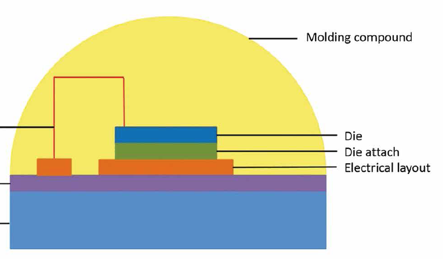
A new chip-on-board (COB) LED-array technology has proliferated broadly in the past few years, enabling enhanced optical properties. For example, Samsung introduced several new COB lines in mid-2015 with significant white-light and color-quality innovations. We investigated the thermal behavior of this type of LED package, to compare their effectiveness with traditionally used materials. We also measured and simulated the influence of geometric parameters of the electrical layouts on thermal resistance. Figure 1: Structure of a high-power COB-LED package
Figure 1 shows the structure of a high-power LED in a chip-on-board package. The majority of the heat from the die is transferred to the outside by conduction. Most of the heat is conducted downward because the thermal conductivity of molding compounds (such as epoxy or silicone), is much smaller than that of the die-attach material (for example, silver conductive adhesive). Thermal conductivity and the geometrical structure of the interface materials greatly influence the heat flow. We used a thermal-impedance test system, the Mentor Graphics T3Ster, to measure the results when the thermal conductivity or structure was changed.
 Figure 2: Structure function of an LED package
Figure 2 shows the structure function of an LED package after the evaluation of the measurement. The structure function presents all the thermal information of the tested LED-package, including thermal resistance in K/W and thermal capacity in Ws/K. Every layer of the thermal capacity represents one kind of material in the LED package. We were particularly interested in the thermal resistances of different materials and their ability to facilitate cooling of the electrical components. A lower thermal resistance translates into better overall performance.
How Electrical Layout Affects Thermal Resistance
The electric layout, the electrical connection between the chip and external electrodes, plays an important role in operation of an LED package, which is why we built different geometrical structures of the electric layout and analyzed them from a thermal perspective. Copper as a connector is the first choice to the manufacturers because of its good electric conductivity and cost. In addition to changing the size of the surface, we changed the thickness of the layout to 35, 70, and 105 μm. Copper has a high thermal conductivity of 385 W/mK. For a copper layout with a surface area of 5 x 5 mm and a thickness of 35 μm, the thermal resistance through the material is
Rth = l : λ·A = 0.0036 K/W
This value is so small that tripling the thickness to 105 μm leads to only a 0.01 K/W change. So why the concern over thickness? The answer lies in the effect of heat spreading, which is not represented by the formula above, but rather detected in measurement results. Figure 3 shows the approach of the effect by using a refraction model [1].
 Figure 3: Heat spreading at different thicknesses of electrical layout
The die’s heat flow reaches the copper layer and then is spread in the material. Compared to optics, the refraction at the boundary surface is dependent on the refraction index, which is the conductivity in the thermal picture. The chip’s junction to a highly conductive material results in a high refraction angle α, so that a high spreading effect should appear. By increasing the copper layout’s thickness, the surface A, through which the heat passes, gets larger. Now, we can calculate the next thermal resistance with the simple formula again. The experimental results and transient thermal simulation with Mentor Graphics thermal simulation software, FloTHERM, are shown in Figures 4 a&b.
Structure functions (measurement data), (b) Simulation data (variation of the thickness)") Figures 4 a&b: (a)Structure functions (measurement data), (b) Simulation data (variation of the thickness)
Figures 4 a&b: (a)Structure functions (measurement data), (b) Simulation data (variation of the thickness)
Both the experimental and simulation results confirm that the total thermal resistance with a thicker copper layout is lower. That is because heat flows into the dielectric through a higher effective surface area (Figure 3). So the dielectric presents a smaller thermal resistance. A higher thermal capacity should be observed because a thicker thickness means more material.
Very thin layers take a long time to simulate, and so the thicknesses of glue and dielectric are different for the test devices. The trend of lower thermal resistance and higher capacity by enlarging the copper layout’s thickness appeared in both the measurement and simulation data.
Testing and Analyzing New Dielectric Materials for Comparison
The dielectric substrate materials we used were based on polymer and/or ceramic materials. We used a non-standard technique to connect the dielectric layer with the board’s substrate and electrical layout. The usual method is to laminate the electrical layout on a ceramic-filled polymer with an epoxy adhesive. However, because the thermal conductivity of a polymer is lower than that of ceramic, we used a ceramic layer that consists of nano-crystalline aluminum oxide crystals (Al2O₃) [2]. We laminated the electrical layout on this pure ceramic layer or used a metallization process for direct contact.
 Nanotherm LC (laminated circuit) and (b) ceramic paste") Figures 5 a&b: Comparison of (a) Nanotherm LC (laminated circuit) and (b) ceramic paste
Figures 5 a&b: Comparison of (a) Nanotherm LC (laminated circuit) and (b) ceramic paste
We tested samples with the same LED package, but different dielectrics, using the thermal impedance measurement system. We directly compared a thick-film nanotherm metal-clad PCB substrate (Nanotherm LC) and a ceramic paste (Figures 5 a&b | Figures 6 a&b), as well as a thin-film nanoceramic substrate for PCBs (Nanotherm DM) and a ceramic-filled polymer [3]. Figures 7 and 8 show the results of the measurement’s structure functions.
 Nanotherm DM (laminated circuit) and (b) ceramic-filled polymer") Figures 6 a&b: Comparison of (a) Nanotherm DM (laminated circuit) and (b) ceramic-filled polymer
Figures 6 a&b: Comparison of (a) Nanotherm DM (laminated circuit) and (b) ceramic-filled polymer
We concluded that the combined thermal resistances of the dielectric and substrate materials are what build the main part of the total thermal resistance in the investigated LED-package. The use of a laminated nano-ceramic instead of a ceramic paste reduced the thermal resistance from 40 to 10 K/W (Figure 8). One reason for this is the small thickness of the ceramic layer (10 μm). The direct comparison of pure nano-ceramic with a laminated ceramic-filled polymer of a standard PCB also shows a reduction of the dielectric’s thermal resistance of about 33%. The conductivity is higher and the thickness of the direct metallized material is smaller, so the consequence must be a reduction in the total thermal resistance.
 Figure 7: Structure functions of Nanotherm LC and a ceramic paste as dielectric material
 Figure 8: Structure functions of Nanotherm DM and a ceramic-filled polymer
Conclusions
This exercise was useful because not every transient thermal behavior can be covered by a simple one-dimensional example. The electrical layout directly affects the measurement curves and must be considered by other models. We concluded that changing the PCB’s dielectric substrate material has the biggest effect on the total thermal resistance of the LED package. In the future, the aging behavior and reliability of both materials are interesting aspects that should be studied.
References:
[1] David P. Kennedy. “Heat conduction in a homogeneous solid circular cylinder of isotropic media”. Product Development Laboratory, Data Systems Div., International Business Machines Corp, Poughkeepsie, NY, 1959.
[2] http://www.camnano.com
[3] Datasheet from Excelitas Technologies and Cambridge Nanotherm.
