Cost and Performance Optimization of Thermal Management Solution for High Power LEDs by Cambridge Nanotherm
The LED industry has a challenge. General lighting requires very bright LEDs that can replace incandescent and halogen lights. Manufacturers need efficacy, cost and manufacturability to be “just right” but most leading solutions, especially in thermal management, are short of the mark. Giles Humpston, applications engineer, Cambridge Nanotherm, discusses ways to combine performance with reasonable costs and good manufacturability.
The LED industry is being challenged. General lighting is where growth is, particularly in the retrofit and automotive markets, and what those markets require is very bright LEDs that can replace incandescent and halogen lights.
There are a number of ways to achieve this, and one of the most ubiquitous is using high-brightness packaged LEDs (HB LEDs). Whilst the lines are blurred, and changing as technologies develop, generally any LED over 1 W can be considered high-brightness.
As LEDs get brighter they also get hotter, so within these packages there will be some form of thermal management designed to conduct the heat away from the die as quickly as possible. Without adequate thermal management the life of the LED is significantly limited - not good when longevity is a key selling point of a product.
The Challenges
The major LED manufacturers continue to push the boundaries by producing larger and brighter LED die (>1 mm.). The question is how to package these to meet the demands of the industry. Traditional leadframe packaging (albeit often with new materials) are a popular choice and essentially offer a direct copper connection to the LED die, producing a very thermally effective and cheap solution.
However there are a couple of issues that rule out leadframes in many HB LED packaging applications. Notably there’s a significant thermo-mechanical mismatch between the leadframe and the die (CTE and Young’s modulus) that can have a significant impact on the reliability of the device. Also, the package size is (relatively) large (>20 mm.).
As a result, the industry is increasingly looking to alternative options like ceramic substrates to package their HB LEDs.
The Requirements
There are a number of requirements that a substrate must meet to be used for LED packaging.
The precision of the circuit needs to be very high. This limits the circuitization process to thin-film direct plated copper (DPC) processes rather than conventional thick-film reductive processes. Generally most HB LED package substrates have the copper tracks sputtered in place as this ensures the tracks are as even as possible (the copper is built up at a 90° angle to the board). This means that the track and gap specification can be much tighter (75 μm and 50 μm respectively for 75 μm copper) - a critical factor when contacts are required for multiple die and your total circuit size is less than 10 mm.. The requirement for thin-film processing limits the range of materials that can be used - generally excluding any type of metal material that has a polymer dielectric layer.
Packaging substrates require through-hole connections that connect the two sides of the circuit together. These are filled with copper during the thin-film processing, so need to be electrically isolated from the rest of the substrate, and have a very small diameter (as small as 130 μm for laser-drilled holes) to speed manufacture. This significantly limits the range of substrates that can be used (standard metal core PCBs fall down again at this point as it’s a very expensive process to create isolated through-holes). These through-holes are also used as thermal vias to help improve the thermal performance of the substrate (copper being a fantastic conductor).
The substrate itself needs to be thermally conductive enough to remove the heat from the LED die to ensure it doesn’t overheat. Here, there is a critical balance between cost and performance.
The substrate price correlates closely with its thermal conductivity; as thermal performance increases so does the cost. In an ideal world the material’s performance would be ‘just good enough’ and the price would reflect this, providing the most cost-effective option within the specified window of thermal performance. The material also needs to be electrically isolating, although as packaged LEDs are not connected directly to mains power this generally only needs to be a maximum breakdown voltage of 500 V.
 Figure 1: Performance and price of technical ceramics
The Current Commercial Options
Currently two materials make up the vast majority of HB LED substrates; Al₂O₃ (alumina) and AIN (aluminium nitride). These two related materials are both from the advanced ceramics family and are used throughout the electronics industry. There are other alternatives that are coming to market and these will be dealt with later in this article.
Core to the use of ceramics is that they tick all of the requirements: They are thermally effective, electrically isolating, drillable, and capable of going through thin-film processing.
Al₂O₃ (alumina, or aluminium oxide) is a chemical compound of aluminium and oxygen. It’s a naturally occurring material and is used to produce aluminium metal, as an abrasive, as a refractory material and as a substrate for electronics. Depending on purity Al2O₃ offers a thermal conductivity of between 20-30 W/mK (and sometimes a little more or less). This makes it an acceptable material for HB LEDs. But only just. The key driver with Al₂O₃ is the cost - it’s a relatively affordable option, particularly when compared to the alternative; its cousin aluminium nitride.
AIN (aluminium nitride) is a synthesized material that is used almost exclusively in the electronics industry. Much like Al₂O₃ it is an excellent dielectric, but unlike Al₂O₃ it is thermally an excellent conductor with a performance (depending on purity) in the region of 140-180 W/mK. However due to the exceptionally high temperatures required to process AIN it is also very expensive.
The industry is crying out for a product that sits between these two materials, one that is ‘just right’ and not too extreme - not too high in thermal performance or too low, not too high a price or too low. This is the sweet spot: a material that provides the ‘just right’ thermal performance between Al₂O₃ and AIN at an intermediate price (Figure 1).
Trial and Error
The first question that comes to mind is why isn’t there a solution to fill this gap? If this is such a big issue surely it would have been addressed by now. The answer is that there have been many attempts.
MCPCBs (metal core PCBs) are sheets of metal such as aluminium or copper coated with a ceramic-infused epoxy dielectric layer. They come in at a composite thermal conductivity of anywhere up to 100 W/mK and cost a fraction of the price of Al₂O₃. On first appearance this makes MCPCBs a good candidate. Unfortunately MCPCBs cannot have electrically isolated through-holes or vias (at least not within a sensible price range). Equally these PCBs are unsuitable for thin-film processing and use thick-film reductive processes to fabricate circuits - way off the fine tolerances required by packaged LEDs. The epoxy also limits the maximum sustained operating temperature of the PCBs and it has a glass transition temperature that gives rise to a number of failure modes.
Si (silicon) is another much touted option. Weighing in at 150 W/mK, it offers good thermal conductivity and there is the entire semiconductor industry infrastructure available with a plethora of established processes available for metallizing it and fabricating vias. But silicon sheets are only available as round wafers, not the rectangular tile formats used in the LED industry. Silicon, like alumina and aluminium nitride, is also quite brittle which results in losses during manufacture and limits the mechanical mounting methods that can be used. Using bolts to fasten down a silicon substrate is not an endeavour for the faint-hearted! Finally there is cost. There is so much demand for high purity silicon from the semiconductor industry that no one bothers to make cheap substrate material. What you can buy is way over specified for LEDs, and this is reflected in the price tag. Similarly most off-the shelf equipment for processing silicon wafers is designed to specifications far beyond what is required and virtually every bit of kit seems to have a price tag north of $1M.
BeO (beryllium oxide), also known as beryllia, is another contender. It’s an effective electrical conductor with a higher thermal conductivity than any other non-metal except diamond. Thermally it actually exceeds most metals. In theory BeO is the perfect material; in practice it’s ridiculously expensive and in dust form is carcinogenic and may cause chronic Berylliosis.
There are also a number of companies, large and small, offering innovative ‘mechanical’ solutions to the problem. Generally these have low adoption because either the design is specific to a given LED die, or it requires the LED to have internal dielectric isolation of its thermal pad.
AIN is an expensive option for a number of reasons: The raw powder is expensive and it undergoes costly non-aqueous processing. It also requires a separate binder removal process; a batch sintering cycle, and a batch flat fire cycle.
There are developments underway to drive down the cost by using a spray drying process, where molten aluminium is sprayed into a nitrogen atmosphere where it reacts to form AIN powder. This has an impact on the performance as well as the price - producing an AIN substrate that comes in a 100 W/mK.
Another prospect is low-temperature sintering of AIN using additives to reduce the temperature and hence process costs. Current endeavour allows the material to densify at 1675°C - 1690°C as compared to 1820°C - 1835°C. Its properties are very similar to traditional AIN except that the thermal conductivity is around the bottom end of performance. Thus far, neither of these low cost variants of AlN have entered the high volume commercial market.
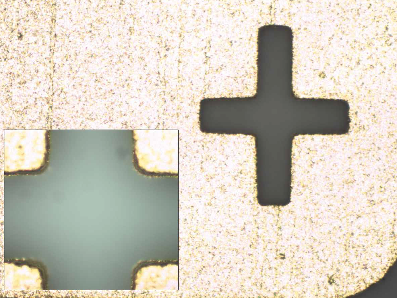
 surface finish. The gap width on this type of feature is typically 75μm. The inset shows a 50x close up of the same thin film substrate that demonstrates the extremely high tolerance achieved") Figure 2: A 10x close up of a circuit feature made using a thin film process with an electroless nickel immersion gold (ENIG) surface finish. The gap width on this type of feature is typically 75μm. The inset shows a 50x close up of the same thin film substrate that demonstrates the extremely high tolerance achieved
Figure 2: A 10x close up of a circuit feature made using a thin film process with an electroless nickel immersion gold (ENIG) surface finish. The gap width on this type of feature is typically 75μm. The inset shows a 50x close up of the same thin film substrate that demonstrates the extremely high tolerance achieved
The ‘Just Right’ Solution
This still leaves a gaping hole in the market between Al₂O₃ and AIN and this is where many are touting an innovative new approach to this problem; nanoceramic.
The new unique material with a composite thermal conductivity of 152 W/mK - perfectly meets all but the most extreme HB LED requirements.
This material is created using a patented Electro Chemical Oxidation (ECO) process that converts the surface of standard grade aluminium into an exceptionally thin (nanoscale) layer of Al₂O₃ measuring no more than a few microns thick. The Al₂O₃ surface forms an integral part of the aluminium so there’s a perfect connection between the different materials. This means heat will conduct fast and easily, whilst the Al₂O₃ can be grown to exactly the right thickness to match the breakdown voltage requirements of the HB LED (Figure 2). The aqueous electrochemical processes used in manufacture are cheap, particularly, as in this case, as the effluent is so benign that it can be discharged directly into the domestic sewer (with a permit from the relevant Utility company!). Thus the material costs are not much more than the base aluminium alloy sheet.
This material also overcomes the problem of many other solutions; the inability to provide through-holes. In this case the aluminium can be drilled (either by laser or mechanically) prior to the nanoceramic conversion process. This means that through-holes and vias will have exactly the same electrical isolation as the surface (Figure 3).
 Figure 3: A cross section of a copper-filled via in a nanoceramic board. The dark lines between the orange copper and the light grey aluminium delineate the nanoscale layer of alumina acting as the dielectric layer
As the surface of this material is a ceramic (Al₂O₃) it is suitable to be put through thin-film DPC processing, ensuring that the circuit has the tolerances needed for HB LED packaging.
With a composite thermal performance of 158 W/mK nanoceramic sits closer to AIN than Al₂O₃ and its price reflects this. This makes nanoceramic the ideal choice for a wide range of HB LED packaging applications, offering the perfect balance of price and performance for all but the most thermally challenging applications.
And there are additional benefits to be had. Unlike brittle ceramics and silicon substrates, aluminium is tough. Nanoceramic, being a nanograin material, also has high fracture toughness. If necessity dictates nanoceramic-coated aluminium plates can even be bent without loss of dielectric isolation. More interestingly, nanoceramic-coated aluminium can be manufactured in huge tiles. The largest AIN tiles on the market today measure a mere 5x7 inches (125x175 mm). Aluminium plates can be purchased with dimensions in metres so can be made in sizes to suit the thin film process line, not the abilities of the ceramic tile manufacturer. Ultimately this means more circuits per tile, helping to bring some of the economies of scale enjoyed in PCB land to semiconductor processing.
Conclusions
HB LEDs rely on ceramic substrates for their construction. The choice is limited to cheap alumina with poor thermal performance or very expensive aluminium nitride with exceptional thermal conductivity. Consequently there is huge demand for a new substrate material that has good thermal properties, competitive pricing and is compatible with the existing LED packaging infrastructure. Nanoceramic coated aluminium admirably meets this specification with the added benefit of being exceptionally tough so there are no yield losses due to breakage. Nanoceramic coated aluminium also offers the tantalising prospect of dramatically increasing the size of LED substrates to exploit the consequential economies of scale.
