Flexible OLEDs for Lighting Applications by the Holst Centre
While OLEDs already have successfully found their way into display applications, the breakthrough in lighting applications is still pending. The reasons are diverse, but cost is one major point. Another reason is the current edge of inorganic LEDs giving reasonable design opportunities in many standard applications. However, there are applications where OLEDs could score, especially the flexible OLEDs. But even these OLEDs need to become cheaper to be applied widely. The Holst Centre and partners aim to develop generic technologies for large area flexible OLEDs which can be processed with roll-to-roll (R2R) technology. Process Engineer Tansim Baig gives an example and an overview of the current status of the development.
In collaboration with our industrial and academic partners, Holst Centre aims to develop generic technologies for large area flexible OLED lighting, including thin film water barriers, which can be processed with roll-to-roll (R2R) compatible technology with high yield. This presentation/ article will give an overview of the key technological developments that are required in order to realize such devices. Highlights from our work will be presented, including devices on plastic and metal foil substrates with solution processed multilayers deposited using our R2R line, large area transparent electrodes including printed metal grids, techniques for light extraction in flexible devices and state-of-the-art thin film flexible water barrier performance (black spot free flexible OLEDs after more than 2000 hours in 60°C/90%RH accelerated lifetime conditions). We will demonstrate flexible devices with comparable performance to glass-based commercially available devices.
Introduction
Organic Light Emitting Diodes (OLEDs) have gathered a lot of interest both from industry as well as academia since their discovery. Today, OLEDs are being used in displays of handheld mobile devices and for general lighting. Flexible, lightweight and with large area emissions in almost any shape, OLEDs will let us do more with light than ever before – opening up new designs and applications. And with lighting currently using around 20% of the world’s electricity, OLEDs’ potential for high efficiency could save huge amounts of energy and greenhouse gas emissions. Holst Centre, and its partners bring together expertise on technologies such as flexible barriers, and large area printing to realize ultrathin, flexible, large-area and moisture-resistant devices.
 Figure 1: Cost comparison for different encapsulation strategies with their advantages and disadvantages [1]
Barrier Foil by the Kilometer
Thin-film devices such as OLEDs and OPVs are very sensitive to moisture, so need a water barrier layer. Traditionally, glass/metal lids have been used to seal the OLEDs / OPVs on a rigid substrate and this resulted in higher lifetime but was expensive and difficult to scale up to large areas. Then came the approach to thin film encapsulate the device which meant reduced costs, improved scalability to larger areas and most importantly lifetime comparable to glass encapsulated devices. At the Holst Centre we are developing a low-cost, large-area thin film based barrier technology based on a SiN-organic-SiN stack which offers sufficient environmental protection to fulfill lifetime specifications of OLEDs / OPVs depending on the application. Most important is to keep in mind the scalability of the process for large area flexible lighting modules. The following diagram gives an overview of barrier encapsulation strategies vs cost.
 Figure 2: Pinhole-pinhole coupling leading to black spot growth in the device [2]
Industry has widely adopted the multi-stack water barrier approach for encapsulation of flexible electronics but the main challenge has always been to avoid the pinhole-to-pinhole moisture diffusion. If the pinholes were coupled, that would create a faster channel for the moisture to seep into the device, thereby degrading the device and leading to the growth of black spots. The thin film, optically transparent water barrier developed at Holst Centre used in combination with metal cathode for top encapsulation of OLED devices on glass substrates has an overall water vapor transmission rate of 10-9 g/m2/day. This results in shelf lifetimes under accelerated shelf life conditions of 60°C/90% relative humidity of more than 4000 hours (approximately 10 years under normal conditions). For flexible OLEDs with a water barrier both above and below the device, shelf lifetimes under accelerated 60/90 conditions are already more than 2000 hours and research to improve this is underway. For flexible OPV devices, we have observed no drop in efficiency of the devices after testing for 7000 hours under 85/85 conditions, which should correspond to more than 60 years under normal conditions. The following plots give more information about the performance of OLEDs and OPVs when tested under accelerated shelf life conditions of 60°C /90% relative humidity and 85°C/85% relative humidity respectively.
 Figure 3: Black spot growth rate in OLEDs with different generations of Holst Barrier technology [1]
For high-volume flexible applications, the barrier must also be flexible and mass-producible. Holst Centre and its industrial partners have developed a roll-to-roll system for barrier production. And in the last year (2013), the collaboration produced 1.4 km of a first generation of the barrier foil (just a single Silicon nitride layer), with an overall (including pinholes) water vapor transmission rate (WVTR) lower than 10-5 g/m2 per day. This is already good enough for PV applications. To develop the roll-to-roll system, the team had to optimize a number of complex issues including web handling, particle contamination, layer homogeneities and the hardware itself. The next goals are to achieve even higher barrier performance by depositing the full barrier stack, increase yields and boost productivity, targeting 300 m of barrier foil per day in a truly industrial-scale process.

Figure 4: Plot showing feasibility study for S2S processed Holst Centre barrier technology for OPVs [1]
Flexible Lumiblade
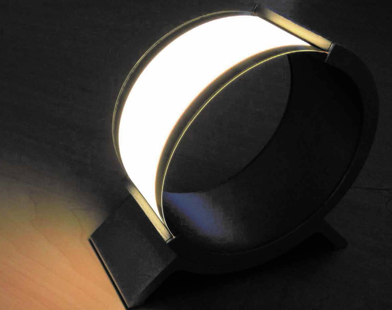
Flexible OLED panels will enable stunning new lighting designs. In 2008, Philips took the first commercial steps in this direction with the launch of the Lumiblade OLED, a glass-based, non-dazzling light source sold as a component for integration into any design. Now, Philips and Holst Centre have developed a flexible version of the Lumiblade. With a 120 mm x 40 mm active area and thickness of just 0.2 mm, these demonstration devices deliver flawless white light at efficiencies of 47 lumens-per-Watt – comparable with glass-based Lumiblades. The flexible Lumiblade consists of a single polymer substrate with the small molecule evaporated OLED (processed in vacuum) sandwiched between two water barrier layers. The flexible Lumiblade device shows no signs of degradation after more than 2000 hours of accelerated lifetime testing at 60°C and 90% relative humidity. Work is ongoing to improve light outcoupling and the compatibility of the substrate with industrial process flows. Figure 5 shows the demonstrator that was developed in close collaboration with our partners
 Figure 5: Flexible Lumiblade made in collaboration with Philips, Dupont Teijin Films, Rolic Technologies, Roth & Rau and Holst centre [2]
Solution-processed R2R OLEDs
Roll-to-roll (R2R) solution processing using slot-die coating is a very attractive candidate for manufacturing OLEDs and organic photovoltaic (OPV) modules mainly because with this approach low-cost large area lighting models can be realized in high volume with costs per square meter lower than €100. We have been able to control the layer thickness and uniformity during slot-die coating and drying to give the 30 -100 nm layer thicknesses required for OLEDs with only a few nanometers of layer thickness variation over the device area [3].
 Figure 6: R2R processed Top-emission OLED on Metal foil measuring 8 cm x 8 cm. Inset: R2R processed Bottom-emission OLED on Metal foil measuring 17 cm x 25 cm
For a number of years Holst Centre has demonstrated the feasibility of making OLEDs on both plastic and metal foil substrates. In 2013, Holst Centre and its industrial partners made significant improvements in process conditions to boost device quality and yield. Using metal foils, researchers fabricated R2R solution-processed top-emissive OLEDs measuring 8 cm x 8 cm Through inspection and optimization of each step of the process flow – including material deposition, patterning and packaging – we improved conditions such as processing speed, layer uniformity and contamination control. The fabricated device showed performance equivalent to small area (2 cm x 2 cm) sheet-to-sheet (S2S) processed devices.
Research on this process will continue at the new Solliance fabrication line in 2014 (a new R2R line aimed to improve throughput and yield of the solution processed devices), leading eventually to volume manufacturing in a production environment and affordable flexible electronics. This new line will enable cleaner fabrication of the devices and is equipped with two slot die coating stations making it easier to coat multiple layers in the same run. The new R2R line has been installed and first tests on the line have already begun.
 Figure 7: Solliance R2R Line
Conclusion
In order to realize the full potential design freedom of OLEDs for lighting at Holst Centre, we are developing robust S2S and R2R flexible water barrier technologies that will allow flexible devices with a long lifetime. We are also developing large area R2R solution processing equipment, and processes in order to produce such devices at low cost and large volume. We have demonstrated the potential of these technologies, by fabricating flexible and solution processed OLED demonstrators with very good performance.
Acknowledgements:
Holst Centre would like to acknowledge support from our industrial partners and from local, national and European funding.
References:
[1] H. Akkerman, proceedings from ICCG10 (2014)
[2] J. Wilson, proceedings from LOPE-C (2014)
[3] J. Gabel et.al proceedings from ICCG9 (2012)
