Hermetic Polymer-Free White LEDs for Harsh Environments
AlGaInN-based white LED can easily achieve lifetimes of up to 100,000 h depending on junction temperature and current density. However, state of the art silicone encapsulated LEDs with powder-based phosphors reveal a strong dependence of field lifetimes on environmental conditions such as humidity, corrosive gas and air pollutant exposure. Dr. Michael Kunzer, Group Leader LED Modules at Fraunhofer Institute for Applied Solid State Physics and his colleagues, Ralf Schmidt, Andreas Zibold, Vasileios Georgiou-Sarlikiotis, Michael Arnold and Isabel Kinski propose luminescent ceramics as an interesting alternative to polymer-dispersed phosphors. This provides entirely new opportunities for the manufacturing of white LEDs. The authors explain the properties and advantage of this hermetic, light converting cap material and how to completely avoid polymers.
White LEDs can achieve lifetimes of several 10,000 h depending on junction temperature and current density. However, state of the art polymer-encapsulated LEDs with powder-based phosphors reveal a strong dependence of field lifetimes on environmental conditions such as humidity, corrosive gas and air pollutant exposure. An interesting alternative to polymer-dispersed phosphors are luminescent ceramics. The development of such ceramic phosphor wafers for LED conversion with diameters of up to 100 mm is demonstrated. They can be manufactured impermeable, provide a 30 times higher thermal conductivity and are chemical, mechanical and temperature resistant. To facilitate this, Fraunhofer has developed high-power LEDs which use luminescent ceramics as hermetic, light converting cap material. Since pollutants cannot penetrate inside and give rise to corrosion, a direct application of these new LEDs without elaborate external housing in chemical burdened environments is possible. As a further advantage the inevitable heat generated by the light conversion is dissipated through the thermally conductive ceramics itself, rather than further burdening the LED chip. This allows high ambient temperature operation. Furthermore, the developed wafer-level package technology allows long device lifetimes with low color drift by completely avoiding polymers.
Introduction
Thermal issues
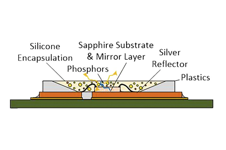
During the last few years phosphor conversion white light emitting diodes (LEDs) based on the AlGaInN-thin-films [1] have replaced traditional light sources in most lighting applications with market shares of up to 80%. Under optimal conditions these white LEDs can achieve lifetimes of up to 100,000 h [2] depending on junction temperature and current density. However state of the art silicone encapsulated LEDs with powder-based phosphors reveal a strong dependence of field lifetimes on environmental conditions such as elevated operation temperature, humidity, corrosive gas and air pollutant exposure. The reason behind this is the design of current white LEDs. They consist of blue light emitting chips and yellow phosphor, which is excited by the blue light and in total produces white light. The yellow phosphor powder is dispersed in a polymer or silicone matrix with low thermal conductivity either placed in a layer directly on, or in a lens above the chip [1]. The packaging of a standard white converter LED is shown in figure 1.
Continuous improvements of the LED chips enable increasing current and luminance densities, which lead to an extreme photo-thermal strain on the phosphor powder and the surrounding polymer matrix even without external influences. This is particularly enhanced since the stoke-losses in the phosphor, when converting blue to yellow light, are unavoidable and the chip surface on which the phosphors settle is already the hottest area in the LED device.
Gas permeability of LED packaging materials
Gas permeability and inertness are important factors for encapsulation and packaging materials. The He gas permeability of different materials over time and versus material thickness is shown in figure 2 for materials commonly used in opto- and microelectronic packaging. The pollutant has to diffuse through the encapsulation first, before being able to reach the silver reflector, p-contact or converter. Thus, the encapsulation should be as impenetrable to gases as possible. Phenyl-and methyl-based silicones are widely used as encapsulation materials for LEDs. Phenyl-based silicones offer a ten times lower gas permeability and at the same time a higher optical index than methyl-based silicones, which facilitates light extraction of the generated light. Methyl-based silicones are general purpose encapsulation materials and are used because of their lower price compared to Phenyl-based Silicones. Epoxy is also used as an encapsulation material. It shows lower gas permeability and a high thermal stability but its low optical index is unfortunate for an LED encapsulation material since this reduces the light extraction efficiency [3]. On the other hand, glasses, ceramics and metals have an up to 10 orders in magnitude lower gas permeability which facilitate true hermetic operation.
![Figure 2: Helium permeability of different packaging materials over time and thickness [8]](https://www.led-professional.com/media/resources-1_articles_hermetic-polymer-free-white-leds-for-harsh-environments_figure2.jpg/@@images/image-0-f2c9d26996e068feda32965ea0a20ce2.jpeg "Figure 2: Helium permeability of different packaging materials over time and thickness [8]") Figure 2: Helium permeability of different packaging materials over time and thickness [8]
Figure 2: Helium permeability of different packaging materials over time and thickness [8]
Effects of trace gases and air pollutants on LEDs
The presence and concentration of air pollutants depend on the application. Especially lighting applications in the heavy and chemical industry, harsh environments, automotive, agriculture and pools can be affected. Also, applications where one would not suspect an accelerated degradation might be concerned, since critical chemical substances are ubiquitous. They are even found to accumulate in the luminaire assembly itself, especially if sealed, since cables and electric components can leak out gases during operation. Penetrating pollutants can accelerate browning and corrosion inside the LED package [4, 5]. This can reduce the lifetime, cause light losses inside the package and cause color shifts that the eye can easily recognize when comparing different LEDs. The silver-based reflectors inside the package and the LED chip itself are particularly sensitive in this respect. For example, the effects of the corrosive pollutant H2S on a mid-power LED with silicone encapsulation are discussed below [6, 7]. In the upper part of figure 3 a mid-power LED operated in room temperature air for 380 h is shown. When the device is operated under the same conditions in air with 10 ppm H2S trace gas a severe darkening of the metal reflector and the bond wires is observed. Furthermore, the silicone matrix above the chip is clouded. For this particular LED a 70% light loss is measured.
 and in air with 10 ppm H2S trace gas (right)") Figure 3: Degradation of a mid-power LED due to operation in pure air (left) and in air with 10 ppm H2S trace gas (right). The diffusion of the corrosive trace gas causes a darkening of the metal reflector and a clouding of the silicone matrix above the chip [6]
Figure 3: Degradation of a mid-power LED due to operation in pure air (left) and in air with 10 ppm H2S trace gas (right). The diffusion of the corrosive trace gas causes a darkening of the metal reflector and a clouding of the silicone matrix above the chip [6]
Ceramic Phosphor Development
To solve the problem of thermal degradation, an entirely inorganic converter with a high thermal conductivity is in the focus of research and development. One approach to prepare such a converter is to sinter a polycrystalline ceramic based on YAG phosphor powder [9, 10]. Polycrystalline YAG ceramics for optical application were described first by Ikesue et al. [11] in the middle of the 1990s by mixing Al2O3 and Y2O3 powders using vacuum sintering. These first ceramics were clearly transparent with about 80% transmittance for visible light without any dopant. In the following years, the YAG was doped with neodymium and the resulting ceramics were used as laser material with properties comparable to YAG:Nd single crystals [12]. Nowadays, instead of phosphor-in-silicone composites, polycrystalline YAG:Ce ceramics, with different levels of transparency, mounted on top of a blue-emitting LED are described for high-power white LEDs [13]. Compared to the phosphor-in-silicone composites the ceramic phosphors have a lower concentration of the expensive cerium dopant, and in addition, exhibit excellent optical and thermal stability. The optical properties and the content of scattering centers can be engineered by varying the degree of porosity, the grain structure, and the minority phases [14]. But the main advantage compared to silicone-based converters is the high thermal conductivity of the ceramic (>5 W/mK) that allows an efficient dissipation of the heat caused by the Stokes losses within the phosphor, thus diminishing the thermal effects on the optical performance. Most recently, the optical properties of transparent, polycrystalline YAG:Ce ceramics were discussed in the literature and Raukas et al. [14] described that the intrinsic scattering by pores induces backscattering, thus leading to absorption within the converter or the LED chip, which should be reduced to achieve a maximum optical conversion efficiency (CE). On the other hand, scattering is required for a homogeneous mixing of transmitted blue and converted yellow light and can be achieved by extrinsic scattering at a rough or structured surface. In combination with a blue (460 nm) LED and under the requirement that 35 percent blue is transmitted to create white light with 5000 K color temperature, the calculated theoretical maximum optical-optical down conversion efficiency is 283 lm/Wopt [13]. The result published in the literature for the luminous efficacy of a 0.63 mm thick YAG:Ce ceramic disk with 0.1 mol% Ce doping was 73.5 lm/W for the complete LED [15]. The transmittance of this ceramic was about 70 percent in the visible range with a 10% transmittance in the blue absorption band at a wavelength of 460 nm and a grain size of about 10 µm with residual pores on the grain boundaries. The data published so far in the literature report on whether the thickness of the specimen or the concentration is a crucial factor, but the data are mostly not clearly comparable and seem to depend on the individual properties, such as increased optical path length due to pore scattering, of the specimen. To study the influence of dopant concentration and sample thickness, our ceramics have been applied as converters in conjunction with a blue LED and the effects of concentration as well as the thickness of the polycrystalline disks on the optical properties of the resulting PC LEDs have been investigated [16].
![Figure 4: Photograph of translucent YAG:Ce ceramics with 0.5 mm thickness and different content of Ce doping; (a) laying and (b) standing on the background [16]](https://www.led-professional.com/media/resources-1_articles_hermetic-polymer-free-white-leds-for-harsh-environments_figure4.jpg/@@images/image-0-f2c9d26996e068feda32965ea0a20ce2.jpeg "Figure 4: Photograph of translucent YAG:Ce ceramics with 0.5 mm thickness and different content of Ce doping; (a) laying and (b) standing on the background [16]") Figure 4: Photograph of translucent YAG:Ce ceramics with 0.5 mm thickness and different content of Ce doping; (a) laying and (b) standing on the background [16]
Figure 4: Photograph of translucent YAG:Ce ceramics with 0.5 mm thickness and different content of Ce doping; (a) laying and (b) standing on the background [16]
The yttrium-aluminum garnet (Y3Al5O12, YAG) polycrystalline disks were prepared by reaction sintering of yttria (99.99%), alumina (99.999%), and cerium oxide (99.995%) in a ratio of Y:Al of 3:5 and with an addition of a different concentration of cerium oxide of 0.1, 0.5, or 1 mol% percent as well as a sintering aid (tetraethyl orthosilicate) under vacuum at a temperature of 1800°C for 5 h in a furnace with molybdenum lining. The powder mixtures were pressed uniaxially at about 50 MPa and cold isostatically at about 700 MPa to form cylindrical disks. The resulting polycrystalline bulk disks were grinded and polished to the required thickness of around 0.4 mm, depending on the amount of scattering. The microstructure of the completely densified ceramics was dominated by the main phase of Y3Al5O12 with less than 10 µm grain size. The scattering effect of the translucent ceramic is the result of a secondary phase of alumina located at the grain boundaries. Further details on the preparation, the microstructure and the optical properties are described elsewhere [16].
 Figure 5: Color and brightness distribution of a 100 mm YAG:Ce ceramic phosphor wafer in a test setup with 460 nm back-illumination
 and luminance distribution (blue) across a 100 mm ceramic phosphor wafer") Figure 6: Lateral color coordinate drift ∆CCY (red) and luminance distribution (blue) across a 100 mm ceramic phosphor wafer. Compared to a three-step MacAdams ellipse only a small min-max color drift of ∆CCY < 0.01 is observed
Figure 6: Lateral color coordinate drift ∆CCY (red) and luminance distribution (blue) across a 100 mm ceramic phosphor wafer. Compared to a three-step MacAdams ellipse only a small min-max color drift of ∆CCY < 0.01 is observed
In order to facilitate wafer-level packaging using large-sized ceramic phosphor wafers the sintering, condensation and wafering process has been scaled up to demonstrate ceramic phosphor wafers with a diameter of 100 mm. An important measure for production yield and LED color binning is the optical homogeneity of the phosphor wafer. To measure the lateral color and brightness distribution the ceramic phosphor wafer was exposed to a homogenous 460 nm LED back-illumination. The resulting color and brightness distribution are shown in figure 5. The CIE 1931 color coordinates x and y as well as the luminance has been measured across the wafer using a compact spectral radiometer (Figure 6). Compared to a three-step MacAdams ellipse only a small min-max color drift of ∆CCY < 0.01 is observed. Furthermore, the luminance distribution is very stable across a 100 mm ceramic phosphor wafer.
Different methods such as volume scattering and laser surface µ-structuring have been applied to remove wave-guiding and the angular color distribution in the far-field pattern. An example of a Laser surface µ-structure prepared by ultra-short-pulse UV ablation in a YAG:Ce phosphor wafer is shown in figure 7. The structure provides extraction facets to avoid light guiding of the yellow light generated inside the phosphor and to improve the angular far-field pattern. Furthermore, specific dielectric filter and anti-reflection layers have been utilized to improve the conversion efficiency of the phosphor and to reduce light losses and unwanted reflections.
 Figure 7: Laser surface µ-structure in a YAG:Ce phosphor wafer. The structure provides extraction facets to avoid light guiding of the yellow light generated inside the phosphor and to improve the angular far-field pattern
Polymer-Free Full Ceramic LED Fabrication
Ceramic phosphors are already used in LED production [13] as chip-level converters which are polymer-bonded on the LED chip and silicone encapsulated. In this work the intention is to demonstrate power-LEDs where the ceramic phosphor wafer is part of the package and is thermally isolated from the LED chip, providing no further thermal burden. Instead the good thermal conductivity of the ceramic phosphor is used to cool of the heat generated by stokes-losses via the package directly into the heat sink. Furthermore, the hermitic nature of the ceramic phosphor is used to form a hermetic polymer-free LED package. To avoid polymer in the package and to achieve hermeticity all parts of the package are eutectic bonded.
 Figure 8: Schematics of the hermetic full-ceramic LED. The phosphor is recessed from the LED chips and forms a part of the package
The fabrication of the LEDs is based on a wafer-level process with a highly thermal conductive Aluminum nitride interposer wafer, a highly reflective Aluminum oxide spacer and the ceramic phosphor wafer on top. A total of four 3 W power flip-chips are bonded inside the cavity. The outer dimensions of the SMT devices are 4.2×4×1.5 mm (Figure 9).
 Figure 9: Hermetic high-power 4×3 W full ceramic white LED in SMT package with 4.2×4×1.5 mm device dimensions
LED Device Characterization
Extensive optical characterization has been performed on the LED devices to improve the conversion efficiency of the phosphors, to improve the blue emission of the pump flip-chips and to reduce absorption and reflection losses within the package. The luminous efficacy of the polymer-free LED for different drive currents are shown in figure 10. A maximum efficiency of more than 140 lm/W is achieved a low current with 125 lm/W at a drive current of 350 mA. Although this efficiency is commonly achieved with polymer-packaged LEDs it is a very high value when compared to conventional hermetic LEDs in TO-can package.
 Figure 10: Luminous efficacy vs. LED drive current of a polymer-free full-ceramic LED
Conclusions
Lighting applications in demanding, hot, harsh, polluted or corrosive environments reduce the useful lifetime of conventional LEDs in polymer-package. This is due to the low thermal stability of polymers and their permeability to gases. For such applications, hermetic polymer-free LEDs have been demonstrated in this work. The LEDs are based on ceramic phosphor which is part of the package. The rest of the package is also full ceramic with eutectic bonding of the individual parts. A SMT device with 4×3 W electrical power and a footprint of 4.2×4.2 mm has been demonstrated. A high luminous efficacy of 125–140 lm/W has been achieved.
Acknowledgments:
We sincerely thank our colleague Thorsten Passow for scientific discussions and Mrs. S. Liu for electrical-optical LED characterization. This work was financially supported by the Ministry of Science, Research and Art Baden-Wuerttemberg (MWK) through the Sustainability Center Freiburg within the Pilot project "SusLight". The ceramic LED phosphor and package development was funded by Fraunhofer within the WISA Projekt HeraKLED.
References:
[1] P. Schlotter, R. Schmidt, and J. Schneider: Luminescence or blue light emitting diodes. Appl. Phys. A 64, 417 (1997).
[2] K. Gordon, "Lifetime of White LEDs", Building Technologies Program, U.S. Departement of Energy, Aug. 2006
[3] Yole Développement SA, "Thermal Management for LEDs and Power Electronics 2017", pp. 30, p. 172, 2017
[4] P. Singh, C.M. Tan, "Degradation Physics of High Power LEDs in Outdoor Environment and the Role of Phosphor in the degradation process", Scientific Reports, Nature, Issue Date: Apr. 2016, DOI:10.1038/srep24052
[5] Osram OS., "Chemical Compatibility of LEDs", Application Note, Feb. 2015, pp. 14–19 [Online] Available: http://www.osramos.com
[6] Andreas Zibold, R. Schmidt, M. Zechmeister, H. Konstanzer, M. Dammann and M. Kunzer, Accelerated LED-Degradation under Exposure to Air Pollutants, LED Lighting Technologies LpS 2017, S. 510, September 2017, ISBN 978-3-9503209-8-5
[7] Andreas Zibold, R. Schmidt, M. Zechmeister, H. Konstanzer, M. Dammann and M. Kunzer, Accelerated LED-Degradation under Exposure to Air Pollutants, LED Lighting Technologies LpS 2017, S. 510, September 2017, ISBN 978-3-9503209-8-5
[8] R Tummala and E Rymaszewski, "Microelectronics Packaging Handbook", Van Nostrand Reinhold, 1989
[9] S. Nishiura, S. Tanabe, K. Fujioka, Y. Fujimoto, and M. Nakatsuka: Preparation and optical properties of transparent Ce:YAG ceramics for high power white LED. IOP Conf. Ser.: Mater. Sci. Eng. 1, 012031 (2009).
[10] H. Bechtel, P.J. Schmidt, A. Tücks, M. Heidemann, D. Chamberlin, R. Mueller-Mach, G.O. Mueller, and O. Shchekin: Fully phosphor-converted LEDs with Lumiramic phosphor technology. In Proceedings of SPIE, Tenth International Conference on Solid State Lighting, Vol. 7784, 2010; p. 77840W.
[11] A. Ikesue, I. Furusato, and K. Kamata: Fabrication of polycrystalline, transparent YAG ceramics by a solid-state reaction method. J. Am. Ceram. Soc. 78(11), 225 (1995).
[12] A. Ikesue and Y.L. Aung: Synthesis and performance of advanced ceramic lasers. J. Am. Ceram. Soc. 89(6), 1936 (2006).
[13] M.R. Krames, O.B. Shchekin, R. Mueller-Mach, G.O. Mueller, L. Zhou, G. Harbers, and M.G. Craford: Status and future of highpower light-emitting diodes for solid-state lighting. J. Disp. Technol. 3(2), 160 (2007).
[14] M. Raukas, J. Kelso, Y. Zheng, K. Bergenek, D. Eisert, A. Linkov, and F. Jermann: Ceramic phosphors for light conversion in LEDs. ECS J. Solid State Sci. Technol. 2(2), R3168 (2013).
[15] S. Nishiura, S. Tanabe, K. Fujioka, and Y. Fujimoto: Properties of transparent Ce:YAG ceramic phosphors for white LED. Opt. Mater. 33, 688 (2011).
[16] K. Wätzig, M. Kunzer, I. Kinski: Influence of sample thickness and concentration of Ce dopant on the optical properties of YAG:Ce ceramic phosphors for white LEDs, Journal of Materials Research 29 (2014), 19, S.2318–2324
