How to Increase the Efficiency of Two-Stage Drivers
In this article, Dr. Weirich from Infineon Technologies, describes a simple method for increasing the efficiency of drivers that can operate with LED engines with a wide range of current and power levels, at virtually no effort. In addition, the method allows for using smaller inductors in the buck stage, leading to lower cost and potentially, smaller size.
LED drivers based on two-stage topologies are much favored thanks to their excellent performance when it comes to input power quality, wide dimming range, and a high quality of light. For power output levels of up to about 50 W, it is extremely popular to combine a PFC flyback and a constant current output buck as a second stage. Such an approach allows for optimization of virtually all aspects of the application since the combination increases design freedom compared to a single-stage driver. However, achieving very high efficiency can be challenging for two-stage topologies. The presented method gives a higher efficiency at no added cost nor design complexity. Moreover, it allows the usage of a smaller inductor value and size in the buck, leading to more compact designs.
LED Drivers and the Quality of Light
Quality of light, first and above all, means the absence of any lighting artefacts, e.g. flicker and stroboscopic effects. Both are caused by modulation of the LED current and should be as small as possible. That means that the design goal for good light quality is an output current that is as close as possible to pure DC under all operating conditions. Any modulation generated by an AC component of the driver output will be detectable in the light output with a negative impact on the quality of light. Currently, there is no mandatory standard for such lighting artefacts, but the maximum light modulation levels given in IEE1789-2015 are a reasonable guide. [1]
A second important aspect comes up when the driver is dimmable. In that case, the lowest dimming level is an important performance indicator and the conformity of this level between different drivers is central. In other words, the lowest dimming level must be highly accurate. What is extremely important is the absence of any light artefacts caused by this low output power condition. Low dimming levels are often implemented by discontinuous LED currents either by using PWM modulation or by going in discontinuous mode of the output stage. Both will cause some modulation of the light and might reduce the light quality.
Now let's consider the requirements for the input side of the driver. International standards, such as IEC 61000-3-2:2014 [5] demand a high power factor (PF) and low harmonic content (THD) of the input current. Essentially, this means that the input current is exactly in phase with the input voltage and that it has a precisely matching waveform, i.e. no distortions. IEC 61000-3-2:2018, the 2018 edition of the above-mentioned standard [6], is applicable for input power ratings above 5 W and addresses dimmable drivers in more detail than before. Briefly, the requirements for input power quality seem to be extremely difficult to meet with a converter that needs to manage proper LED driving as well.
Consequently, single-stage drivers are dropping in popularity and are increasingly replaced by two-stage solutions. They make it much easier to optimize the first stage for an excellent power quality over a wide range of output powers. The second stage is then fed with a reasonably stable DC voltage and can be optimized to provide a clean and stable supply current for the LEDs.
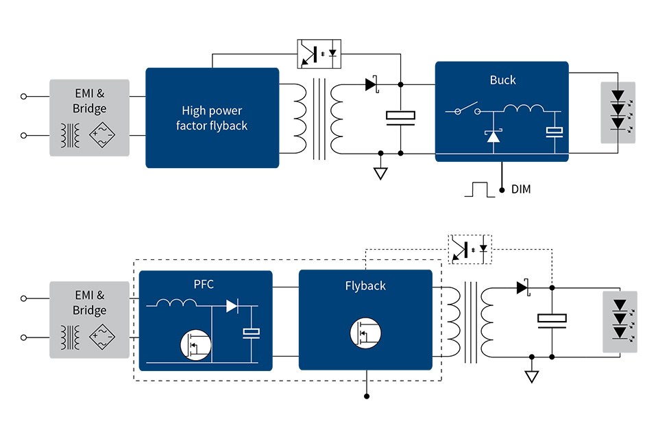
As depicted in figure 1, there are two basic configurations for two-stage drivers: galvanic isolation after the first or after the second stage. It is obvious that the second configuration is not well suited for applications that demand more than one output channel, for example, tunable white or RGB solutions. It may also be a disadvantage in some single output channel applications where, in the second solution, the dimming interface is not isolated from power line. All this is completely independent of whether a primary side regulation (PSR) or a secondary side (SSR) is used.
We can conclude that two-stage LED drivers based on an isolated PFC followed by a buck stage are the most versatile solution for power levels up to about 50 W and maybe even somewhat higher. That explains why the topology has become extremely popular for high light and power quality LED drivers.
System Efficiency
The described two-stage solution presents challenges for designers as well. Achieving very high efficiency is one of them. This can be illustrated by a simple example. If the first stage achieves an efficiency of 92%, which is an excellent value for a flyback, and the buck has 97%, the system efficiency will be slightly above 89%. Considering the upcoming EU directive for lighting, the Single Lighting Regulation (SLR), which will replace several previous regulations and will demand an efficiency of at least 85% for a 50 W driver, there seems to be a comfortable margin. Many driver manufacturers nevertheless consider higher efficiencies as important, especially since that would result in lower cooling effort in an often thermally critical environment. Consequently, they have their own standards such as minimum efficiency of 88%, a number heard often. It needs to be emphasized that this efficiency level is desired over a wide load range, not only at maximum load.
There are a bunch of known measures to increase efficiencies of both stages. But all these measures considerably increase the complexity and cost of the driver. In case of a hysteretic buck, such as Infineon's ILD6150 or ILD8150, combined with an SSR flyback like XDPL8218, there is a simple solution to increase efficiency. This solution consists simply of a changed arrangement of the feedback circuit. With this new arrangement, the output voltage of the flyback becomes variable while the difference between flyback and LED output voltage is regulated.
Hysteretic Buck Efficiency Increase
One thing worth mentioning is that the hysteretic buck is an almost perfect solution for the second stage of a LED driver. Deeper insights on hysteretic buck operation are provided in the application note on ILD8150 80 V high side buck LED driver IC with hybrid dimming.[2]
Further details of the theory of operation of hysteretic bucks are readily available for an interested reader in [2].
 Figure 2: Schematic of hysteretic buck with ILD8150
Its operation principle is perfectly suited to provide constant output current since there is no feedback loop needed to stabilize this current. No feedback loop implies that no loop-compensation is needed either. Consequently, the hysteretic buck is unconditionally stable under all normal input and output conditions. Finally, as the schematic in figure 2clearly shows, component count is small, especially if the MOSFET is integrated.
Key to understanding the idea behind the proposed efficiency improvement is the fact that the hysteretic buck is operating with variable switching frequency fS. This switching frequency is determined by the value of the inductor L, the amplitude of current ripple i, and, finally, input and output voltages VIN and VOUT.
Why is the switching frequency fS so important? Simply because it dominates the losses in a hysteretic buck and, in turn, the efficiency. As can be taken from [2] and [3], total conduction loss (i.e. the sum of conduction loss of MOSFET and diode) is governed by their respective resistances and by the LED current. On the other hand, switching loss is heavily dependent on VIN as well as fS.
Analysis in [2] reveals that the difference VIN - VOUT between input and output is the dominant term in the expression for fS and that the variation of the latter is much lower, if the difference VIN-VOUT is kept constant, as illustrated in figure 3.
With a fixed VIN (blue curve), the frequency rises rapidly with a falling LED voltage and almost triples when the output voltage drops by one third. Consequently, not only will the switching losses of the buck rise by a factor of almost three, but also the losses in the inductor will increase by a similar factor. What the fixed VIN curve (blue curve) shows is that the selection of a suitable inductor is not an easy task. The value of the inductor needs to be small enough to keep the switching frequency above audible range under all conditions but must not allow fS to go too high in order to limit the losses. Switching frequencies higher than 150 kHz may cause issues with conducted EMI as well.
When the difference VIN-VOUT is kept constant (yellow curve), the behavior changes completely. The frequency is linearly going down with the LED voltage. That implies that the inductance can be reduced considerably, say halved, while still having lower switching frequency in the majority of the operating range. In case the size of the inductor is kept the same, a lower inductance means lower turns and less losses. But it may be even more appealing to a designer to use a smaller inductor size and value. The red curve in figure 3 has been calculated with an inductor value that is 2.5 times lower (340 µH) than what is the case for the other two curves (860 µH). That still leads to pretty moderate frequencies, all below 85 kHz in this case, which are extremely unlikely to cause any EMI issues. We can expect that the efficiency improves greatly in most parts of the load range and that there is a prospect for reduction of inductor size, leading to a more compact design and lower cost.
, fixed VIN-VOUT (yellow), and fixed VIN-VOUT plus 2.5 times lower inductance(red)") Figure 3: Variation of switching frequency vs. VOUT of a hysteretic buck with fixed VIN (blue), fixed VIN-VOUT (yellow), and fixed VIN-VOUT plus 2.5 times lower inductance(red)
Figure 3: Variation of switching frequency vs. VOUT of a hysteretic buck with fixed VIN (blue), fixed VIN-VOUT (yellow), and fixed VIN-VOUT plus 2.5 times lower inductance(red)
Implementation
The developed concept is surprisingly simple to implement. Instead of stabilizing the output voltage of the flyback stage, as shown in figure 4 (top), the difference of the input and output voltages of the buck is regulated to a constant value of e.g. 5 V(Figure 4 - bottom). This regulation mainly needs a restructuring of the feedback network so that almost no additional components are needed, except for some low-cost resistors.
 Figure 4: Standard feedback configuration and proposed new configuration
Extensive theoretical analysis has been carried out to prove that such feedback configuration does not cause any issues with loop stability [4]. For both, the PFC flyback and the hysteretic buck, the small signal transfer functions have been determined and loop stability analysis has been implemented using MATLAB/SIMULINK. As expected, we found that this type of feedback does not cause any stability issues other than those known from a traditional circuit. Loop response needs to be slow and loop bandwidth needs to be below approximately 20 Hz, as with any other PFC flyback. At the same time, this feedback configuration does not cause any negative impact on the performance of the buck. It is also worth noting that neither ripple suppression nor load response is affected negatively.
How small a difference in VIN-VOUT can be made is an important question for many designers. This is determined by the maximum duty cycle of the buck.
In CCM, duty cycle d is always
d = VOUT/VIN
Thus,
VIN = VOUT, Max/ dMax
This finally leads to the equation:
VIN-VOUT ≥ VOUT, Max (1/dMax-1)
ILD8150 has a maximum duty cycle dMax of 0.97. If the selected maximum output voltage is e.g. 60 V, the minimum difference VIN-VOUT can be as small as 2 V, leading to extraordinary small inductors.
Results & Conclusions
The expected efficiency improvement has been validated in a system consisting of an AC-DC converter based on XDPL8218, followed by a hysteretic buck based on ILD8150. This system is described and fully documented in [2]. In the first tests of the proposed solution only the feedback configuration has been altered, exactly as described above. Nothing else has been changed for this first validation. The system efficiency and its increase by altering the feedback circuit is shown in figure 5. While at maximum output voltage (16 LED ≈ 48 V), the increase in efficiency is 1.3%, reaching more than 3% at lower output voltages (11 LED ≈ 33 V).
Even more exciting are the results displayed in figure 6. Here we changed the output inductor of the buck - a relative bulky 860 µH through-hole device was replaced with a 100 µH surface mount. Although the latter has an almost five times smaller volume (1.4 cm³ versus 6.4 cm³) and a similar factor in the weight (7 g versus 32g), the efficiency is almost identical.
 Figure 5: Increase of system efficiency by changing the feedback configuration vs. output voltage
 vs. 100 µH SMD inductor (green)") Figure 6: Comparison of system efficiency with altered feedback configuration and original 860 µH inductor (red) vs. 100 µH SMD inductor (green)
Figure 6: Comparison of system efficiency with altered feedback configuration and original 860 µH inductor (red) vs. 100 µH SMD inductor (green)
This is an impressive result because it is possible to increase efficiency while at the same time volume, weight, and cost are reduced.
References:
[1] IEEE Recommended Practices for Modulating Current in High-Brightness
LEDs for Mitigating Health Risks to Viewers, IEEE Standard 1789-2015,Jun. 2015.
[2] ILD8150 80 V high side buck LED driver IC with hybrid dimming
[3] ILD8150 high-frequency operation
[4] Thomas Altmann, Efficiency Optimization, Size and Cost Reduction of a LED
Driver, Master Thesis, Technische Universität München, 2019
[5] IEC 61000-3-2:2014 Electromagnetic compatibility (EMC) – Part 3-2: Limits –
Limits for harmonic current emissions (equipment input current ≤ 16 A
per phase), 4th edition, 2014
[6] IEC 61000-3-2:2018 Electromagnetic compatibility (EMC) - Part 3-2: Limits -
Limits for harmonic current emissions (equipment input current ≤16 A
per phase), 5th edition, 2018
