InGaN Nanowires Make Light Mixing Efficient and Smart
The correlated color temperature (CCT) of high color rendering index (CRI) LED lighting systems can, in principle, be tuned over a wide range. As an alternative approach to conventional phosphor based LEDs, a full-color LED array consisting of red, green and blue (RGB) InGaN based nanowire LEDs monolithically integrated on a micro-scale level has been proposed and fabricated. J. Lee from the Nano Electronics Lab at the Samsung Advanced Institute of Technology, Renjie Wang, Hieu P. T. Nguyen, Ashfiqua T. Connie, Ishiang Shih, and Zetian Mi from the Department of Electrical and Computer Engineering at McGill University in Montreal explain how this technology works and how the three multi-color subpixels on the same chip can be separately biased and can exhibit full-color emission which can be tuned controllably in a wide CCT range.
The conventional incandescence and fluorescence lamps are limited in terms of their efficiency, lifetime, and environmental impact. The wide usage of solid-state lighting sources is expected to significantly reduce the electricity consumption for lighting, and reduce greenhouse gases and other pollutions accordingly. Currently, high power LEDs can already compete with conventional light sources. LED-based solid-state lighting sources have also been widely applied for signals and displays. To improve the resolution, optimal viewing distance and color rendering of displays, the technique of subpixel rendering has been commonly used. However, the current phosphor-based white LEDs have been criticized for its low CRI and Stokes fluorescence loss. An alternative approach is to monolithically integrate RGB LEDs directly on a single chip, enabling the tuning of the spectral power distribution. Such a phosphor-free approach can lead to color-tunable LEDs with low power consumption, extremely small size, and high CRI. However, the lack of suitable lattice-matched substrates for the growth of high-In content quantum wells leads to extremely low efficiency of GaN-based LEDs in the wavelength range > 560 nm, severely restricting the device performance including the luminance and tunability of CCT [1]. Moreover, some previously reported approaches for achieving multi-color emission, including the use of vertically stacked multiple quantum well LEDs have significant drawbacks, including the light absorption by adjacent narrow bandgap quantum wells and poor heat conduction.
Compared to conventional planar quantum well devices, nearly defect-free III-nitride nanowire LED heterostructures can be grown directly on lattice mismatched substrates and can exhibit outstanding device performance and reliability. To date, with the use of InGaN nanowire structures, high-efficiency emissions across the entire visible spectral range have been demonstrated [2-4]. In this context, we have developed laterally arranged RGB LEDs consisting of various InGaN nanowire structures, which provides a high-efficiency approach for subpixel rendering, significantly improving the color rendering index and broadening the color tunability. These monolithically integrated, monochromatic micro-LED arrays, with their sizes in the micron or even sub-micron scale, can readily generate tunable, multi-color emission for lighting and full-color displays.
Growth and Fabrication
To control the composition and dimensions precisely in the atomic level, radio frequency plasma-assisted molecular beam epitaxy (MBE) was used for the growth of nanowires in this work. MBE has reached a high level of maturity and now offers several important advantages for InGaN LEDs compared to the MOCVD growth method, such as in-situ monitoring capability, better interface control and lower growth temperature for the incorporation of high indium compositions. Compared to other material growth/synthesis techniques, MBE can provide the highest control of the structural, electronic, and optical properties of various nanostructures. In addition, the realization of p-type doping in GaN is more efficient in an MBE growth environment, compared to MOCVD [5]. The unique self-catalytic nanowire growth process we have developed can also minimize the formation of extensive surface defects and unintentional impurity incorporation.
In this work, self-organized InGaN/GaN dot-in-a-wire LED heterostructures were grown directly on n-type Si substrates under nitrogen-rich conditions. The use of large area Si substrate, compared to conventional sapphire substrate, can significantly reduce the substrate cost and improve the throughput. The LED structure consists of ~ 0.4 μm GaN:Si, ten vertically aligned InGaN/GaN quantum dots, ~ 10 nm p-doped AlGaN electron blocking layer (EBL), and ~ 0.2 μm GaN:Mg. Each InGaN/GaN dot consists of ~ 3 nm InGaN, which is subsequently capped by a 3 nm GaN barrier layer. Our group has previously demonstrated high performance InGaN/GaN dot-in-a-wire LEDs with green, yellow, red and phosphor-free white light emission [6-10]. In this work, such InGaN dot-in-a-wire LEDs, with emission wavelengths in the range from ~ 450 nm to 700 nm, were grown on a single Si wafer using a three-step selective area growth process. As shown in figure 1, three different sets of laterally arranged multi-color InGaN/GaN dot-in-a-wire LED arrays were grown in sequence on a large area Si substrate. For each nanowire LED, the emission spectrum can be readily tailored by varying the sizes and/or compositions of the dots by simply varying the MBE growth conditions.
Illustrated in figure 1(a), a selectively patterned SiOx dielectric layer, with designed microscale openings, was first created on Si substrate by standard photolithography and etching techniques. Blue nanowire LEDs were first grown on the patterned substrate, shown in figure 1(b). The SiOX mask was then selectively removed, illustrated in figure 1(c). A SiOX layer was then used to cover the blue LED nanowire subpixels formed on Si, which is followed by the creation of additional opening apertures for the growth of the 2nd step (green/yellow) LED subpixels at desired locations, shown in figure 1(d). Subsequently, the 3rd step orange/red LED subpixels were grown on patterned Si substrates using a similar process, shown in figure 1(e). Finally, illustrated in figure 1(f), the SiOX mask and nanowires on SiOX were removed to reveal the three-step nanowire LED arrays. Through extensive studies, we have confirmed that the regrowth steps do not have any negative effect on the quality of the previously grown LED structures. The SiOX dielectric layer works well to protect the previously grown nanowires from subsequent growths and fabrication steps. Figure 1(g) shows the optical image of the three-step nanowire LED subpixels corresponding to figure 1(f). The three-step RGB arrays were positioned next to each other and sorted in this order as illustrated to enable the seamless integration and light mixing of multi-color LEDs on the chip-level.
 Figure 1: A three-step growth process of multi-color InGaN nanowire LEDs
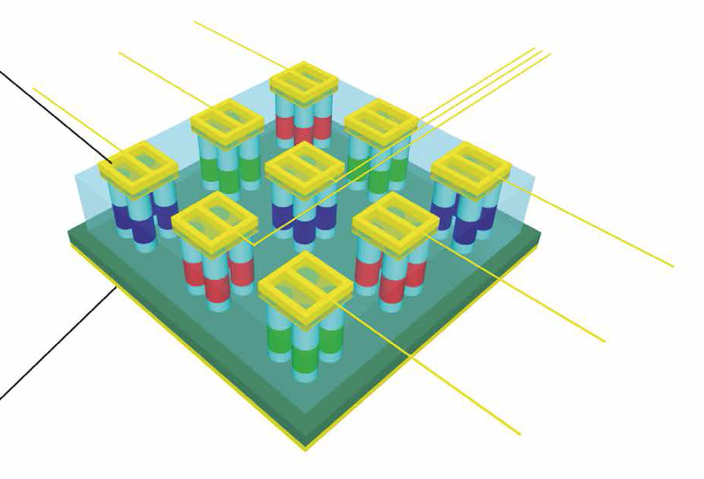
Subsequently, nanowire LED devices with areal sizes of 300.300 μm2, 100.100 μm2 and 50.50 μm2 were fabricated. The RGB pixel size can be readily scaled down to the sub-micron scale. Schematically illustrated in figure 2, p- and n- contacts were deposited on the top surface of nanowires and the backside of the Si substrate, respectively. In this study, the multi-color InGaN LED devices exhibit excellent current-voltage characteristics, including relatively low series resistance (~ 20 Ω or smaller).
High CRI and Tunable CCT
In the LED arrays, each full-color LED pixel consists of three multi-color subpixels, which can be separately biased and can exhibit strong emission in the blue, green/yellow, and orange/red spectral range. Consequently, light mixing at the chip level can be readily achieved. More importantly, by varying the injection current to each LED subpixel, the spectral power density and the CCT can be controllably tuned.
 Figure 2: Schematic of a multi-color nanowire LED array
Shown in the figure 3(a), tunable electroluminescence (EL) emissions across the entire visible spectral range (~ 450 nm to 700 nm) can be achieved on a single Si wafer. Moreover, for each growth step, the peak position and spectral linewidth of the EL emission, e.g., the green and yellow EL spectra obtained in the 2nd step, and the orange and red spectra in the 3rd step, can be further engineered by varying the growth conditions, thereby providing a great level of flexibility in tuning the emission color of the integrated LED arrays and also leading to full-color LED chips tailored for specific applications. Moreover, each single LED device can be made to exhibit a broad spectrum, due to variations of In compositions in the dots, providing a phosphor-free approach for achieving high efficiency orange, red, or even white light emission with high CRI values.
 emissions, The output spectra of a representative triple-color LED pixel") Figure 3 a&b: Tunable electroluminescence (EL) emissions, the output spectra of a representative triple-color LED pixel
Figure 3 a&b: Tunable electroluminescence (EL) emissions, the output spectra of a representative triple-color LED pixel
We have shown that the laterally arranged nanowire LED pixels can exhibit color-tunable characteristics of varied CCTs in the range from 1900 K to 6800 K by independently applying injection current to each LED subpixel. Such monolithically integrated tunable full-color LED arrays also display very high CRI (>90). The output spectra of a representative triple-color LED pixel consisting of blue, green and orange/red subpixels are shown in figure 3(b). It is seen that by adding green and orange/red light components, the CCT can be varied from ~ 6500 to 3800 K. For the operation at CCT of 3826 K, the CRI can be as high as 90.7.
Figure 4 shows the summary of the emission characteristics of three different triple-color LED pixels, which were grown under different conditions. It is seen that the CCT values can be varied from ~ 1900 K to 6800 K. Very large CRI values (> 85) can be achieved for devices with warm and neutral white light emissions (CCT < 5000 K). The output characteristics of these devices are further shown in the CIE chromaticity diagram, illustrated in the inset of figure 4.
 Figure 4: The summary of the emission characteristics of three different triple-color LED pixels
High Efficiency and High Onset of Droop
A wide color-tunable range can be achieved at various output power levels. Previously, the achievement of high internal quantum efficiency (~ 60%) InGaN/GaN dot-in-a-wire green, yellow, red and white LEDs has been reported at room temperature [6,7,8,11]. An output power of more than 5 mW was also reported for an unpackaged InGaN based nanowire LED by us [12]. Moreover, the presence of droop under these measurement conditions is relatively small, which is consistent with previous studies on InGaN/GaN green, yellow, red and white nanowire LEDs on Si(111) substrates [6-12]. It has been reported that no efficiency droop was observed for injection current up to ~ 480 A/cm2 for red nanowire LED [6] and up to ~ 2,000 A/cm2 [9] for white nanowire LEDs.
Future Research Demands
One drawback of the current design is the light absorption by the underlying Si substrate. It is worthwhile mentioning that today’s high brightness LEDs are achieved by removing the underlying sapphire substrate. For practical applications, the underlying Si substrate may be selectively removed by wet chemical etching process to improve the light extraction efficiency. Previously, we demonstrated that nanowire LEDs grown on Si substrate can be readily transferred to Cu substrate [13], which can eliminate any optical absorption by the substrates and further provide much more effective thermal management. It is also of interest to fabricate monolithically integrated sub-micron scale multi-color nanowire LED and laser arrays on transparent substrate for enhanced light extraction efficiency, directionality, and output power. Such sub-micron scale nanowire LED arrays can be realized by utilizing a combination of nano-imprinting lithography and the afore-described selective area MBE growth process.
Industrialization Perspectives
These miniaturized RGB nanowire LED arrays are well suited for future smart lighting, display, and imaging applications. Such nanowire devices can be readily fabricated in the sub-micron or nanoscale and can also be integrated with Si electronics for applications in projection displays, imaging, and biochemical sensing. The process of making such nanowire devices, including MBE growth and fabrication, only incurs a few hundred dollars per 3’’ wafer in the lab level. The cost can be dramatically reduced by utilizing a multi-wafer MBE production system. Using high-resolution lithography techniques, the pixel size of the RGB InGaN/GaN dot-in-a-wire LEDs can be further reduced to ~ 100 nm or smaller. These nanoscale LEDs will be well suited for ultrahigh-resolution display and imaging applications. Based on this work, it is also of interest to develop monolithically integrated color-tunable nanowire surface- and edge-emitting lasers to achieve high power coherent light sources on Si that can operate in the entire visible spectral range, enabling the development of high-performance color-tunable miniaturized laser sources for high brightness and high-resolution displays.
References:
[1] T. Mukai, M. Yamada, and S. Nakamura, “Characteristics of InGaN-based UV/blue/green/amber/red light-emitting diodes,” Jpn. J. Appl. Phys. 38 (7A), 3976–3981 (1999)
[2] H. Sekiguchi, K. Kishino, and A. Kikuchi, “Emission color control from blue to red with nanocolumn diameter of InGaN/GaN nanocolumn arrays grown on same substrate,” Appl. Phys. Lett. 96 (23), 231104 (2010)
[3] K. Kishino, K. Nagashima, and K. Yamano, “Monolithic integration of InGaN-based nanocolumn light-emitting diodes with different emission colors,” Appl. Phys. Express 6 (1), 012101 (2013)
[4] R. Wang, H. P. T. Nguyen, A. T. Connie, J. Lee, I. Shih, and Z. Mi, “Color-tunable, phosphor-free InGaN nanowire light-emitting diode arrays monolithically integrated on silicon.” Opt. Express 22 (107), A1768-A1775 (2014)
[5] S. Zhao, B. H. Le, D. P. Liu, X. D. Liu, M. G. Kibria, T. Szkopek, H. Guo, and Z. Mi, “p‑Type InN Nanowires.” Nano Lett. 13 (11), 5509−5513 (2013)
[6] H. P. T. Nguyen, S. Zhang, K. Cui, A. Korinek, G. A. Botton and Z. Mi, “High-efficiency InGaN/GaN dot-in-a-wire red light-emitting diodes,” IEEE Photon. Tech. Lett. 24 (4), 321-323 (2012)
[7] H. P. T. Nguyen, K. Cui, S. Zhang, S. Fathololoumi, and Z. Mi, “Full-color InGaN/GaN dot-in-a-wire light emitting diodes on silicon,” Nanotechnol. 22 (44), 445202 (2011)
[8] H. P. T. Nguyen, S. Zhang, K. Cui, X. Han, S. Fathololoumi, M. Couillard, G. A. Botton, and Z. Mi, “p-Type modulation doped InGaN/GaN dot-in-a-wire white-light-emitting diodes monolithically grown on Si(111),” Nano Lett. 11 (5), 1919–1924 (2011)
[9] H. P. T. Nguyen, K. Cui, S. Zhang, M. Djavid and Z. Mi, “Controlling electron overflow in phosphor-free InGaN/ GaN nanowire white-light-emitting diodes,” Nano Lett. 12 (3), 1317–1323 (2012)
[10] H. P. T. Nguyen, S. Zhang, A. T. Connie, M. G. Kibria, Q. Wang, I. Shih, and Z. Mi, “Breaking the carrier injection bottleneck of phosphor-free nanowire white light-emitting diodes,” Nano Lett. 13 (11), 5437–5442 (2013)
[11] Y. L. Chang, J. L. Wang, F. Li, and Z. Mi, “High efficiency green, yellow, and amber emission from InGaN/GaN dot-in-a-wire heterostructures on Si(111),” Appl. Phys. Lett.6 (96), 013106 (2010)
[12] H. P. T. Nguyen, M. Djavid, S. Woo, X. Liu, A. T. Connie, S. Sadaf, Q. Wang, G. Botton, I. Shih, and Z. Mi, “Engineering the carrier dynamics of InGaN nanowire white light-emitting diodes by distributed p-AlGaN electron blocking layers”, Scientific Reports 5, 7744 (2015)
[13] H. P. T. Nguyen, Q. Wang, and Z. Mi, “Phosphor-free InGaN/GaN dot-in-a-wire white light emitting diodes on Cu substrates,” J. Electron. Mater. 43 (4), 868–872 (2014)
