Lacquer Systems for PCBs – Optical Requirements and Performance in Applications by Lackwerke Peters
It is common knowledge that the quality of an LED luminaire doesn’t only depend on the LED. However, there are many components and technologies that are not taken into account from the outset. Lacquer systems for circuit carriers is one of them. Dr. Manfred Suppa and Johannes Tekath from the Lackwerke Peters demonstrate the relevance of conformal coatings, solder resists and casting compounds and how they influence LED lighting systems.
Light emitting diodes (LED) are used in a steadily growing number of applications, and it is expected that they will continue to replace conventional light sources in more and more areas. Depending on the usage, reflective, diffusing or light-absorbing properties are required for the printed circuit board as a direct support of LED components, or respectively, for the solder resist forming the surface of the substrate. Furthermore, the necessity of insulating the assembly by conformal coatings or 2-pack casting compounds depends on the later usage of the assembly. The conformal coatings or 2-pack casting compounds should not impair the optical properties of the LEDs in the long run, despite their covering effect. This paper deals with the following aspects of using lacquer systems for circuit carriers in combination with LEDs:
• What are the optical requirements with regard to the substrate surface? How can different conformal coatings, forming the “surface finish“, fulfill these requirements?
• Which classical lacquer technology criteria, tests and evaluation standards can be used for an optical characterization? Are there any specific features that should be considered? What are typical results? These aspects are discussed in detail, in particular with regard to the color stability/yellowing resistance of various white solder resists under different processing and test conditions.
• Are there any specific features in processing these lacquer systems compared to conventional applications? What would the typical approaches for a solution be?
• In which applications may clear-transparent 2-pack casting compounds based on polyurethane be used for “LED covering” even when combined with effect additives? What is the experience gained in the past regarding the long-term stability under various conditions? In this paper, studies on storage temperature and UV and/or weathering resistance will be discussed in detail.
Surface Reflectivity
Bodies either reflect, diffuse or absorb electromagnetic radiation, with these processes depending, amongst others, on the wavelength. With reference to visible light, this means that a body which fully absorbs in the range of 380 to 760 nm does not throw back any radiation provoking a sensation in the eye – this body is black, while a body that sends back all incoming wavelengths (of white light!) appears to be white.
The relevant parameter describing an “optical” surface is the so-called reflectivity, which is defined as the – diffused – light thrown back from a body. While bodies of perfect white have an even reflectivity of 100% for all wavelengths, black bodies do not reflect at all. Perfect grey bodies have an even reflectivity of wavelengths between > 0 and < 100%, while colored bodies display a selective reflectivity, meaning that they absorb a part of the light in such way that the thrown-back light is composed of different wavelengths areas, thus giving the impression of color. Figure 1 shows the reflectivity graph of a photo-imageable solder resist with the reflectivity factor being higher than 90 in the color-relevant spectrum between 400 and 780 nm. Figure 1: Reflectivity graph of white photo-imageable solder resist
Measuring of Colors – Color Metrics
In order to quantitatively describe the color or a color difference, one may illuminate the surface to be measured by a defined light and measure the light that is thrown back, i.e. the reflected light. Mathematical calculations include both the type of light source and the color impression of the eye when measuring “color“. In order to describe a color by specific parameters, the so-called CIE Lab System (more precisely, the L*, a*, b* system of CIE [A]) is usually applied, which is based on transforming the primary calculated color values X, Y, Z into the specific coordinates L* (brightness), a* (red-green-value), and b* (yellow-blue-value). The derivative of the Lab values will not be presented here, referring to [1] as an example.
 Figure 2: Schematic figure of the CIE L*a*b* System and its color coordinates
As a major advantage, the CIE Lab System allows to describe color differences. Δ E* is the index of a color difference i.e. for the sameness or similarity of colors, calculated as spatial Pythagoras from the three values L1* – L2*, a1* – a2* and b1* – b2*:
 For describing a white surface, one may either use the reflectivity graph (Figure 1), or refer to the brightness value L* from the CIE Lab System. Here a perfect white surface is characterized by the coordinates L*=100, a*=0 and b*=0.
The CIE Lab System has the advantage of limiting the parameters to three figures and of defining differences based on these values which correlate, to a large extent, with color sensation.
In the conventional lacquer industry, the method of colorimetric measuring is wide-spread and often used a criterion for specifying the quality of goods to be supplied, or for describing characteristics such as weather resistance or temperature stability.
Besides an evaluation in accordance with the CIE Lab System, there is the possibility of specifying the color change, i.e. the yellowing effect, according to DIN 6167 which is generally used by the paper industry. DIN 6167:1980-01 speaks about yellowing when an undesired yellowing of the material is noticed in consequence of a specific treatment. In this case, a yellowness value G is obtained from the primary values X, Y and Z. The change of this yellowness value between an untreated (G0) to a treated sample (G1) is calculated to give the yellowing index V designated as such.
The color coordinates of the Lab System, i.e. the values L*, a* and b*, can be directly determined by means of colorimeters. For measuring the yellowness index G, special software tools are necessary; should these not be available, this index must be calculated manually based on the X, Y, Z values.
 - (Courtesy of ColorLite GmbH)") Figure 3: Diagram of sensor head adapter with a d/8° geometry (integrating sphere) - (Courtesy of ColorLite GmbH)
Figure 3: Diagram of sensor head adapter with a d/8° geometry (integrating sphere) - (Courtesy of ColorLite GmbH)
Since the ΔE*, ΔL* and Δa* values for describing color distances and/or color changes are widely accepted, it is recommended to use these parameters. A typical L*, a*, b* evaluation of three white solder resists is displayed in figure 4. This description allows a detailed interpretation of color changes through physical measurement in connection with pre-defined values.
 Figure 4: The reflectivity expressed by the L* value of a white solder mask, depending on layer thickness
Colorimeters are composed of a light source, the sensor head with different geometries and a detector such as a spectrophotometer. Among the methods available for measuring, just spectrophotometers are suitable for taking a reflectivity graph in the desired wavelength range of 380 to 760 nm. To determine the color coordinates, two basic test geometries – 45°/0° and d/8° (integrating sphere) – are available, which can be easily combined as shown in the setup (Figure 3). The tests described below have been carried out based on the d/8° geometry and include an integrating sphere with gloss trap.
Both methods outlined above give a value for the difference. The smaller the difference, the yellowing index V or the ΔE* color difference, the lower is the yellowing effect or, respectively, the color change. The subject of yellowing and color measurement is described in detail in [1].
Expressed in ΔE*, the best quality (lowest yellowing) is that < 1. The grading towards lowest quality is shown by the respective color changes displayed in table 1.
 Table 1: Color differences expressed in ΔE* and their general evaluation
Covering Power
Another basic property of colored coating materials is the so-called covering power describing their capacity of hiding the color or any color difference with the substrate. The criterion applied here is the contrast between the contrasting fields of the substrate that is to be agreed upon. As a result of absorption and scattering, the covering power is a function of the coloring pigments. In case of white pigmented coatings, this is just a result of scattering. On the one hand, the covering power is dependent on the layer thickness, on the other it depends on the respective contrast of the substrate and has a characteristic limit. The covering power cannot be adjusted to any thinness of layer; the minimum layer thickness required for an opaque white lacquer in case of a black-white contrast is assumed to be approx. 40 μm. Unlike thermal curing solder resists, UV curing coating materials – including all photo-imageable solder resists – should be slightly transparent if a sufficient UV cross linking shall be ensured down to the substrate.
The physical limits of covering power have to be taken into account in processing: a lacquer applied in a layer of 10 μm looks less white than a 20 μm layer, while a layer of 30 μm, in turn, has a whiter appearance than that of 20 μm layer thickness. At a layer thickness of 40 μm or higher, the white color no longer depends on the thickness, thus the full covering power has been reached. If the color is to be evaluated or measurements be carried out based on a thickness of less than approx. 40 μm, the substrate shall be included in the evaluation. This means that the reflectivity graph and the L* value also depend on the layer thickness.
In figure 5, these facts are shown as an example based on the reflectivity graphs. A white photo-imageable solder resist has been applied and measured on copper in three different layer thicknesses – 20 μm, 48 μm and 60 μm. Here the lower reflectivity at 20 μm layer thickness due to insufficient covering power can be noticed clearly.
Solder Resists on LED Circuit Carriers
With the increasing use of SMD LEDs for illumination purposes and the request for a better luminous efficacy, it is more and more often required that the circuit carrier shall reflect, in an optimum manner, the light bound to fall on it. Reflectivity is defined as the diffuse reflection of radiation (light). In general, the circuit carrier is covered by a solder resist, which, besides electrical insulation and the required chemical resistance, has to fulfill new functions for such applications.
When using a white solder resist, this may be the reflectivity of a background lighting application on the one hand, or high color stability under exposure to sunlight and/or heat on the other.
If a solder resist is white, the simple term “white“ does not fulfill the actual requirement such as an optimum reflectivity. The characteristic of reflectivity is closely connected with the color and can be described through colorimetric measurement as stated above. For this application, very high demands in terms of whiteness, reflectivity and color stability under temperature load and/or sunlight exposure can only be fulfilled by solder resists that were especially developed for this purpose.
 applied on copper, dependent on layer thickness") Figure 5: The reflectivity of a white solder mask (ELPEMER SD 2491 TSW R1) applied on copper, dependent on layer thickness
Figure 5: The reflectivity of a white solder mask (ELPEMER SD 2491 TSW R1) applied on copper, dependent on layer thickness
When processed, solder resists undergo different temperature loads which may visibly affect the (white) color, one of them being the solder process. As a result, a change to the yellow color i.e. yellowing will take place, as shown in figure 6 by means of reflectivity graphs. A white solder resist supplied to an assembly company should undergo the lowest possible color change within subsequent solder processes.
 Figure 6: Reflectivity graphs of both a classical photo-imageable solder resist and one belonging to the new generation, before and after reflow loading
As from the underlying mechanism of formation, there are different causes for yellowing:
• Heat
• Sunlight
• Environmental influence (such as moisture, chemicals)
In this context, yellowing is primarily caused by heat and sunlight, or by accelerated UV radiation simulating sunlight. The yellowing is considered to be light-induced when light rays of a wavelength below 380 nm (UV rays) are thrown on polymers. Through radical-induced photochemical reactions so-called chromophore groups are formed, creating the color effect. Heat-induced yellowing is the formation of such chromophore groups subject to polymers‘ exposure to temperatures > 100° for a longer period of time.
Such a color change can be measured either through the so-called yellowing index or via the color difference in the CIE Lab System.
For characterizing this color change, the above described color difference ΔE* may be used. In case of a pure white surface, the two values ΔL* und Δb* should receive special attention. While ΔL* describes the change of brightness, Δb* characterizes the blue-yellow shift thus yellowing in this case (Figure 2). A low Δ value indicates a high quality of the solder resist’s color stability, with differences smaller than 0.5 being hardly noticeable to the untrained eye.
It was generally found that any color change through the influence of heat – thermal yellowing – is primarily due to oxygen attack. In this way, solder processes without oxygen show less yellowing than those taking place under air exposure; this effect, however, can no longer be noticed visually for the white solder resists of the youngest generation (Figure 7).
") Figure 7: Color change of a solder resist after a reflow process, vapor phase soldering and a long-term storage at different temperatures displayed as Δb (yellowing)
Figure 7: Color change of a solder resist after a reflow process, vapor phase soldering and a long-term storage at different temperatures displayed as Δb (yellowing)
As briefly mentioned above, color metrics are also perfectly suitable for describing the color behavior following long-term exposure to high temperature, and for determining any critical long-term temperature loads. Figure 7 is an impressive example of the shift of the b* yellowing values under different storage temperatures and two solder processes. A shift towards higher positive b* values describes a yellowing effect – in this case, temperature yellowing. As expected, the red-green-values a* have not changed. It can be clearly noticed that long-term temperature resistance is ensured up to 105 °C. A temperature load of 125 °C provokes distinct color shifts i.e. yellowing here. Colorimetric tests of this kind are suitable for measuring color resistance after long-term storage under high temperature, for example in accordance with the IEC 60216 [6] family of standards, and for determining the respective temperature index for optical characteristics.
Figures 7 and 8 further indicate that the yellowing effect occurring in solder processes is less due to temperature, but rather to a combination of temperature and air oxygen; in this way, solder processes under nitrogen show less yellowing than those carried out under a normal atmosphere.
") Figure 8: Colorimetric study of the yellowing behavior of a white solder resist during long-term storage at different temperatures (85°C, 105°C, 125°C)
Figure 8: Colorimetric study of the yellowing behavior of a white solder resist during long-term storage at different temperatures (85°C, 105°C, 125°C)
In these examples, an acceptable temperature load is limited to 105°C; at higher temperatures the yellowing is unacceptable.
The electrical performance is not affected at all by yellowing; previous studies have revealed that there are no changes.
Under the influence of global radiation – commonly known as sunlight – many polymers display more or less distinct degeneration effects. Absorbing in the short-wave range of the visible light, the final products of the so-called photo-oxidation are the cause of yellowing processes of polymers, too. This yellowing effect particularly affects epoxy resins which are commonly used in the production of solder resists. To produce sufficiently light-stable white solder resists, these had to be developed based on a different polymer class.
 UV-LSL: UV curing solder mask LPiSM: liquid photoimageable solder mask 2K-LSL: two-component solder mask") Figure 9: Colorimetric evaluation of UV yellowing by means of the XENON test [B] (1000 h) UV-LSL: UV curing solder mask LPiSM: liquid photo-imageable solder mask 2K-LSL: two-component solder mask
Figure 9: Colorimetric evaluation of UV yellowing by means of the XENON test [B] (1000 h) UV-LSL: UV curing solder mask LPiSM: liquid photo-imageable solder mask 2K-LSL: two-component solder mask
In view of determining the light resistance or, respectively, the yellowing resistance, test specimens may be exposed to outdoor weathering for several years, for example within the so-called Florida test. If results shall be obtained on a short-term basis, one may choose among various accelerated weathering tests, for example the so-called Xenon test. In the frame of this test, the specimen is exposed to the radiation of a xenon arc lamp, the filtered spectrum and the irradiance of which are similar to natural sunlight. Appropriate short-term tests have been described by various DIN standards [2, 3]. According to past experience 250 h correspond, as a rule of thumb, to a one-year natural load. As an example, figure 9 shows colorimetric evaluation results of various solder resists following UV load. In this diagram, the Lab value changes have been given as numbers for simplification.
Clearly noticeable here is the yellowing effect revealed by the distinct change of the Δb value (db), while the brightness shift ΔL is much lower. For the three solder resists used as examples, the UV resistance after the 1000 h XENON test is very good; with the 2-pack solder resist being the most UV stable adjustment by far. Photo-imageable solder resists of the old generation have not been included here since their color changes of much more than 3 are out of question.
As expected, tests that were carried out based on an LED light illumination of 460 nm wavelength during 1000 h reveal no change in reflectivity that is visually noticeable or measurable. Potential influence is not expected from the in falling light, but rather from simultaneous heat input likely to heat up the coating to 100 °C.
Protective Coating of LED Equipped Assemblies
The protective coating can be applied either on the entire circuit carrier, or on those areas left free from LEDs. If the LEDs shall be coated, too, the coating must fulfill, besides an electrical insulation under harsh environmental conditions, the requirement of a high optical performance including, for example, yellowing and gloss stability.
Another option of conformal coating is to use white opaque lacquers and to apply them by the selective coating method leaving LEDs uncoated. This method is suitable for perfectly covering dark components of single-sided LED circuit carriers. Conformal coatings or permanent coatings of this type are characterized by a high light and heat resistance featuring very high reflectivity values. As an example, a CIE Lab value of a white permanent coating for LED circuit carriers R460 is 0.92 for reflectivity, or, in terms of brightness L*, the value 97.
If printed circuit boards assembled with LEDs need to be completely coated for the protection against moisture, such conformal coatings are usually chosen which ensure an electrical insulation in different atmospheres on the one hand, and which, in terms of weathering resistance, display a very low tendency of yellowing under such loads on the other.
The colorimetric values obtained with transparent specimens cannot be compared with the traditional reflectivity measurement of white lacquers, for example. While color measurement of colored coating materials primarily reveals reflectivity characteristics, measuring of transparent materials rather display transmission or absorption properties. During measuring, rays pass through the body and reach the reflecting substrate, and pass on to the measuring value sensor (integrating sphere).
 Figure 10: Demonstration sample of a white covered conformal coating
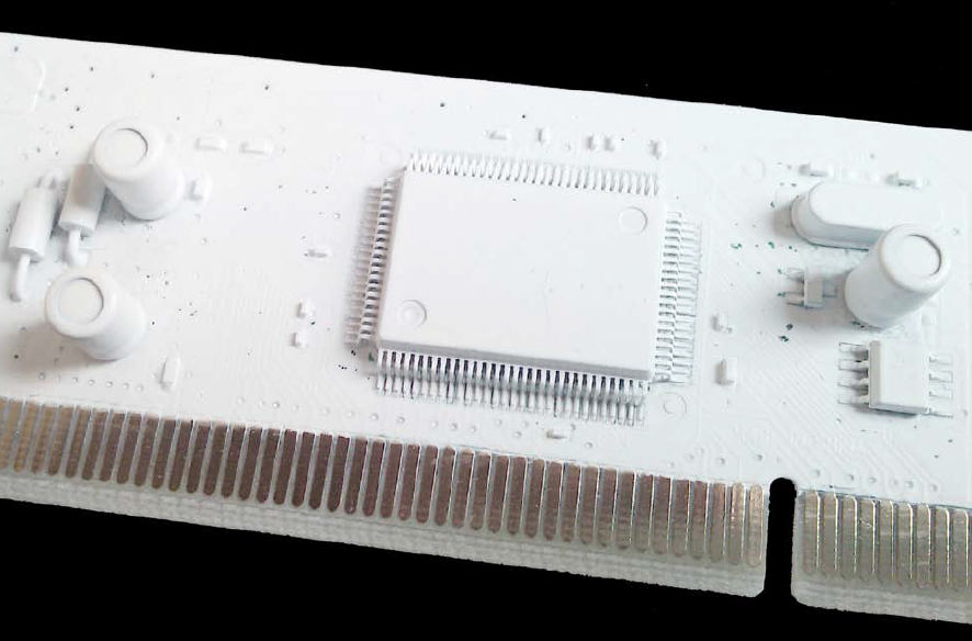
Figure 10 shows an example of a white, covering conformal coating applied on an electronic assembly, displaying the excellent covering power of this type of conformal coatings. Even black components are covered securely. It is understood that these coating materials also fulfill all general requirements placed on conformal coatings.
Conclusion
Thoroughly selected lacquers can increase system efficiency and protects the electronics. It helps to increase reliability, but there are big differences between products and their processing. While one product is very resistant against environmental influences others are not and for instance show yellowing very soon. To make the right selection and to achieve the desired results a close cooperation with specialists is mandatory.
Explanations:
[A] International Commission on Illumination (CIE - Commission internationale de l’éclairage)
[B] Acc. to DIN EN ISO 11341 with suntest CPS+, without humidification, irradiance: 550 W/m.
References:
[1] Loos, Hans, Farbmessung, Verlag Beruf+Schule, Itzehoe (1989)
[2] DIN EN ISO 11341:2004-12, Beschichtungsstoffe - Künstliches Bewittern und künstliches Bestrahlen - Beanspruchung durch gefilterte Xenonbogen-Strahlung
[3] DIN 6167:1980-01 Beschreibung der Vergilbung von nahezu weißen oder nahezu farblosen Materialien
[4] Zuverlässigkeit von fotostrukturierbaren Lötstopplacken bei Belastung durch Temperaturdauer- und Temperaturwechselstress, 14. FED-Konferenz, 21.-23. September 2006 Kassel
[5] W. Berger, Untersuchungen zur Dauerwärmebeständigkeit von Anstrichen, farbe+lack, 72.Jahrg., S. 127-132 (1966)
[6] DIN EN 60216-1; VDE 0304-21:2002-09, Elektroisolierstoffe - Eigenschaften hinsichtlich des thermischen Langzeitverhaltens
