Lead Halide Perovskite Nanocrystals - A New Promise for Light Emitting Devices
Perovskites structured materials have attracted scientific and technological interest in the last four years. Recent studies have shown that these materials could deliver high photoluminescence efficiency at any desired wavelength in the visible spectrum. Mirko Prato and Francesco Di Stasio, Technologist and Marie Curie Fellow of the Institute of Photonic Sciences at the Istituto Italiano di Tecnologia focus on the application in single color LEDs (red, green and blue) and white emitting color-converting layers. They discuss what limits their application in everyday technology like toxicity and limited functional stability.
Perovskites structured materials have attracted great interest for optoelectronics applications in the last four years. Mostly, this is thanks to the promising properties of such materials combined with low cost and solution based processing, which greatly contribute to their high potential for photovoltaic and light-emitting devices (LEDs). Recent studies have shown that these materials could also be obtained as colloidal nanocrystals exhibiting very high photoluminescence efficiency and with the possibility to emit at any desired wavelength in the visible spectrum by tuning their chemical composition and/ or by controlling their size and shape. Even though research on perovskite nanocrystals is still at the starting stage, they are expected to have a significant impact in the development of novel lighting devices in the near future thanks to their facile synthesis compared to other semiconductor nanocrystals. Here, we discuss the latest findings on perovskite nanocrystals light emitting devices. In particular, we will focus on their application in single color LEDs (red, green and blue) and white emitting color converting layers. Furthermore, we will discuss what limits their application in everyday technology, such as toxicity (caused by the presence of lead in their structure and the use of organic solvent for processing), and limited functional stability.
Introduction: The Rise of Lead Halide Perovskites
Lead halide perovskites are quite an old material, already having been synthesized for the first time in 1893[1] and fully characterized from a structural point of view in the late 1950s [2]. Figure 1: Top panel: Crystal structure of cubic lead halide perovskites with the generic chemical formula APbX3
The typical perovskite crystal structure is reported in figure 1. Lead halide perovskites have the chemical formula APbX₃, where A is a monovalent cation and X is a halide ion (either Cl-, Br- or I-). As reported in figure 2, Pb and X ions arrange forming sharing-corners octahedra and the monovalent cation fills the space in between four (PbX₆)4- octahedra. The monovalent cation is typically either an alkali metal (cesium, Cs+) or a small organic molecule as methylammonium (MA, CH₃NH₃⁺) or formamidinium (FA, CH(NH₂)2⁺).
Despite their age, these materials only came to the interest of the optoelectronics community quite recently. Indeed, it was 2009 when, for the first time, Kojima et al. introduced CH₃NH₃PbI₃ (having a direct bandgap of 1.55 eV, which makes this material a good light absorber over the whole visible solar emission spectrum) as sensitizers for solar cells, measuring a power-conversion efficiency of 3.8% [3]. Starting from this germinal work, an increasing number of papers appeared in recent years, reaching the impressive number of 1834 papers dealing with perovskite-based solar cells in 2016 (more than 5 papers a day!); researchers quickly identified challenges that needed to be addressed for these materials to be technologically successful, showing continuous improvements in device architectures and conversion efficiencies, that reached the value of 22.1% [4] in 2016. The results obtained for high-efficiency photovoltaics suggest that lead halide perovskites are excellent semiconductors for optoelectronic devices in general: an efficient solar cell material should also be a good light emitter according to the detailed balance in the Shockley–Queisser formulation [5], where all recombination should ultimately be radiative. Indeed, previous works have shown that perovskites possess strong photoluminescence, making them potential candidates for use not only in solar cells but in light-emitting devices, too [6]. In particular, perovskite nanocrystals (NCs) obtained by colloidal synthesis can exhibit very high photoluminescence quantum efficiency, coupled with narrow emission linewidths and color tuning over the entire visible spectrum.
In this document, we will briefly summarize the latest finding on the emerging field of perovskite nanocrystals. Firstly, we will give an overview of the typical synthesis protocols for these NCs, focusing on the optical properties from a solution. We will also comment on the possibility of tuning the emission color, either by chemical composition or by shape engineering. We will then move to discuss the main results obtained with these NCs in monochromatic LEDs as well as phosphors in white color layers. We will also discuss the issues that are limiting to the implementation of these materials in commercial LED systems.
; rapid increase in perovskite solar cell power conversion efficiency in the same period of time (Source: NREL efficiency chart [4]); comparison of LED external quantum efficiencies in OLED, QLED and perovskitebased LED (PeLED)") Figures 2a-c: Number of scientific publications dealing with solar cells based on perovskite materials in the last 7 years (Source: http://www. scopus.com); rapid increase in perovskite solar cell power conversion efficiency in the same period of time (Source: NREL efficiency chart [4]); comparison of LED external quantum efficiencies in OLED, QLED and perovskite-based LED (PeLED)
Figures 2a-c: Number of scientific publications dealing with solar cells based on perovskite materials in the last 7 years (Source: http://www. scopus.com); rapid increase in perovskite solar cell power conversion efficiency in the same period of time (Source: NREL efficiency chart [4]); comparison of LED external quantum efficiencies in OLED, QLED and perovskite-based LED (PeLED)
Colloidal Synthesis of Lead Halide Perovskite NCs
The first solution-based synthesis of colloidal MAPbBr₃ NCs was reported by Pérez-Prieto and colleagues in 2014 [7]. After this seminal work, researchers around the world have reported several synthesis protocols for perovskite NCs. It is out of the scope of this document to enter into the details of all the different methods, for which we refer the interested readers to the recent review by A. Rogach and coworkers [8].
It is, however, helpful to underline the common points between those methodologies. Indeed, independently on the choice of the monovalent cation (either MA or FA for hybrid organic-inorganic MAPbX₃ perovskites or Cs for fully inorganic CsPbX₃ NCs), most of the protocols rely on the use of long chain organic molecules (amines and/or acids), used to provide a self-termination of the crystallization, leading to the formation of discrete nanoparticles in solution. These solutions (typically in organic solvents) have been shown to be stable over several weeks/months, provided that no polar substances (like water and moisture, for instance) come in contact with the NCs themselves. Due to the ionic character of these perovskites, in fact, the NCs could easily deteriorate if the proper mixture of solvents is not used. This environmental instability is more pronounced for hybrid perovskites, e.g. MAPbI₃ could dissociate into PbI₂ and MAI, the latter of which is volatile [9]. A fully inorganic structure without a volatile organic component is therefore highly desired, especially in view of a possible use of these materials in commercial devices.
The preparation methods for fully inorganic CsPbX₃ NCs can be divided into two classes: the so called “hot injection” and “room temperature recrystallization”. In the “hot injection” approach, PbX₂ powder is dissolved in a mixture of organic solvent an d surfactants. After that, the preheated Cs precursor is injected into the PbX₂ solution at a specific temperature (in the 130-200°C range) and then, NCs form. Their growth is usually arrested by abruptly lowering the reaction temperature with an ice-bath. Even if this approach usually results in NCs of higher quality in terms of crystallinity and size and shape dispersion, the use of high temperatures and controlled reaction atmospheres as well as the needed abrupt temperature change could potentially limit its application for large scale production. On the other side, “room temperature recrystallization” methods could face the requirements of upscaling. In this approach, which can be briefly described as transferring inorganic ions from good into very poor solvents, Pb2+, Cs⁺ and X- sources powders are dissolved completely in a specific solvent together with surfactants. Secondly, a small amount of the above solution is added into a bad solvent. After transfer, the enormous drop in solubility produces a highly supersaturated state immediately, which induces a rapid recrystallization. Surfactants help to control the size and disperse them in various nonpolar solvents. So obtained NCs exhibit comparable optical properties to that of NCs synthesized at high temperatures [10].
The main distinctive character of the optical properties of these NCs could be summarized as follows:
Dependence of the emission wavelength on the halogen (X = Cl, Br or I):
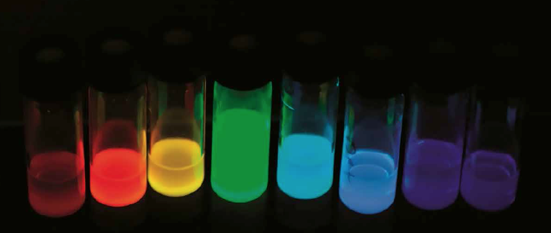
Independently on the choice of the monovalent cation and of the preparation protocol, lead halide perovskite NCs show an interesting dependence of the emission wavelength on the used halide ion. If the size of the NCs is large enough to avoid quantum confinement effects, Cl-based NCs emit in the blue-violet region, Br-based NCs in the green region and I-based NCs in the red region of the visible spectrum. Therefore, using the very same preparation method, and changing only the chemical nature of the halogen, it is possible to obtain the fundamental emitters of the RGB color model.
Narrow emission line-widths:
As in the case of other semiconductor quantum dots, lead halide perovskite NCs are also characterized by narrow photoluminescence line-widths. Typical full width at half maximum values are in the order of 0.1 eV, corresponding to 12-15 nm in the blue-violet, approximately 20 nm in the green and 35 nm in the red region of the visible spectrum [11, 12].
High PL QY:
Furthermore, even without any surface shelling, the lead halide perovskite NCs show quite high photoluminescence quantum yield values. This is true especially for Br- and I-based NCs, for which PLQY of almost 100%[13] and 60-70% [14], respectively, have been reported. Importantly, such high efficiency values are partially retained in films where efficiencies above 30% are observed [15].
On the other hand, Cl-based NCs are typically less luminescent, and PLQY of maximum 10% have been reported.
Tuning of the Optical Properties
A useful property of lead halide perovskite is that mixed-halide compositions are possible. This implies that, by a careful balance of the used halogens, any desired emission wavelength in the 400 – 700 nm range could be targeted and obtained. There are two ways to obtain such a result. The first is to run the colloidal synthesis by combining appropriate ratios of halogen precursors (e.g. PbX₂ salts), as done for instance by the group of M. Kovalenko [12]. Alternatively, it is possible to make use of a peculiar property of perovskites in general, i.e. the mobility of anions (halides, in the present case) in the crystal lattice. In this way, by exposing a solution of CsPbBr₃ NCs to an excess of other halide ions (either Cl or I), we demonstrated that anion exchange reactions occur and Br ions could be replaced partially or completely in the NCs, resulting in a blue shift (adding Cl) or red shift (adding I) of the PL peak. The optical properties (PL linewidth and QY) of the NCs obtained by anion exchange are in line with those of the NCs obtained by direct synthesis [11].
Another interesting venue to control perovskite nanocrystals emission is a typical approach for semiconductor quantum dots, i.e. quantum confinement. By changing the synthesis conditions (such as reaction temperature, acidity of the reaction medium and/or chain length of the organic molecules used as surfactants), researchers have been able to tune the size of the NCs down to the quantum confinement regime [16-19]; in this condition, the band-gap of the lead halide perovskite could be “opened” in a control manner and, accordingly, the PL peak could be blue-shifted. This procedure could be particularly helpful to obtain bright blue emitters based on lead bromide perovskites since, as we discussed before, PL QY values in the blue-violet region of the visible spectrum are typically lower than in the rest of the spectrum.
LEDs for Display Application
LEDs based on perovskites films are still outperforming their NCs counterpart. As an example, in 2015, hybrid organic-inorganic perovskites were used to demonstrate green emitting LEDs with a current efficiency of 42.9 Cd/A [20]. Nonetheless, inorganic (CsPbBr₃) perovskite nanocrystals based LEDs showed an astonishing improvement in performance since their synthesis has been reported at the beginning of 2015. In fact, the first green emitting CsPbBr₃ nanocrystal LED reported a current efficiency of 0.43 Cd/A at the end of 2015 [21], and in just more than a year (end of 2016) these type of LEDs have reached 13.3 cd/A in a similar spectral range [22] (see Table 1). Performance is improving very rapidly thanks to the “know-how” developed in the last 20 years on the fabrication of LEDs using solution processed materials. In fact, most of the fabrication techniques used in organic (OLEDs) or II-VI and III-V semiconductor quantum-dot LEDs (QLEDs) are completely transferrable and nowadays a plethora of different materials that can be used as electrodes or charge transport layers are available, thus facilitating device optimization. Despite the rapid improvement in efficiency and emitted luminance, most of the results reported in literature are limited to the green spectral region (500-550 nm) with only two articles reporting red and blue emitting perovskite nanocrystal LEDs [21, 23]. Red emitting perovskite nanocrystals LED have shown a maximum luminance of 2335 Cd/m2 (current efficiency is not reported in this case). On the other hand, blue emitting perovskite nanocrystals LEDs are still lagging behind in terms of efficiency and maximum luminance.
, turn-on voltage (V), maximum external quantum efficiency (EQE), maximum current efficiency (Cd/A), maximum luminance (Cd/m²), reference and date of publication") Table 1: Overview of representative results on inorganic and hybrid halide perovskite nanocrystals LEDs: electroluminescence peak emission (nm), turn-on voltage (V), maximum external quantum efficiency (EQE), maximum current efficiency (Cd/A), maximum luminance (Cd/m.), reference and date of publication
Table 1: Overview of representative results on inorganic and hybrid halide perovskite nanocrystals LEDs: electroluminescence peak emission (nm), turn-on voltage (V), maximum external quantum efficiency (EQE), maximum current efficiency (Cd/A), maximum luminance (Cd/m.), reference and date of publication
Hybrid-inorganic-organic perovskite nanocrystals based on methylammonium (MAPbBr₃) have been employed as well. This type of LED has shown a current efficiency of 4.5 Cd/A in 2015. Up until now MAPbBr₃ nanocrystals have seen a limited research focus for light-emission applications compared to fully inorganic perovskite ones. This is because replacing MA with inorganic Cs offers the perovskite extra thermal stability up to its melting point (≈500 °C) and promise longer device operational lifetime. In fact, a major issue of perovskite nanocrystals LEDs is their stability and overall operational lifetime. This has been studied marginally compared to the work done for perovskite solar cells and much more work is necessary to shed light on the degradation processes taking place during LED operation, air exposure and their storage (the so called “shelf-life”). For example, the use of mixed halides for color tuning has already been reported to cause unstable emission color after only few seconds of operation [23].
Despite the great improvement in efficiency and luminance for green-emitting LEDs observed in just over one year, much effort is still needed to understand the nanocrystals degradation processes, stabilize their color, fabricate efficient blue and red LEDs and optimize the device architecture. All these represent great challenges while chemists around the world are constantly synthesizing novel perovskite nanocrystals (very recently, for example formamidinium based perovskite green-emitting LEDS have been demonstrated with a current efficiency of 6.4 cd/A [24]). The constant search for new perovskite nanocrystals structures and compositions is motivated by the presence of lead in the crystal. Toxicity of lead based perovskite remain an important limiting factor for commercial application and the hope is that knowledge achieved on the fabrication of LEDs using fully inorganic or hybrid lead perovskite nanocrystals can transferred to their non-toxic counterparts be in the future.
Perovskites Nanocrystals as Phosphors and in Light- Converting Layers
Another venue for application of perovskite nanocrystals is their use as phosphors. More conventional II-VI and III-V semiconductor quantum-dots have already seen successful application in this field in display applications, for example Samsung recently commercialized their first ultra-high definition TV based on Quantum dots. Such technology in display removes the reduced vision angle typical of LCD displays and allows enhanced contrast. Similarly, perovskite nanocrystals have been used for the fabrication of color converting layers but for the generation of white light, mainly thanks to the ease of tuning their color. Phosphor-based solid-state white LEDs provide a much higher efficiency alternative to incandescent and fluorescent lighting. In particular, few relevant examples of perovskite white emitting layers are present in the literature, employing either CsPbX₃ (where X is either Br, I or Cl) inorganic nanocrystals [28, 29], hybrid perovskite nanocrystals, or hybrid methyl and octylammonium meso- to nanoscale crystals [30]. In all cases, researchers have taken advantage of the color tailoring of perovskite by changing the type of halide in their structure or the nanocrystal size/shape. In these applications, perovskites nanocrystals have demonstrated the capability of obtaining color-rendering index above 80 with color temperature in the 5000-6000 K range, similar to currently commercially available white LEDs.
Another interesting application of perovskite nanocrystals as phosphors is in the field of telecommunication. Thanks to their relatively fast photoluminescence lifetime (of less than 10 ns) CsPbBr₃ nanocrystals have been successfully employed as phosphors in a visible light communication system (VSL) [31]. This technology promises to solve the current limitations in data and wireless communication present in conventional IR-based networks. As such, VSL requires fast emitters with a large modulation bandwidth. In the case of the light converter proposed (employing both perovskite nanocrystals and conventional phosphors), the system shows a bandwidth of 491.4 MHz, a value significantly higher than conventional nitride-based phosphors (~12.4 MHz), organic materials (40−200 MHz) or YAG-based phosphors (3−12 MHz), demonstrating once again the potential of perovskite nanocrystals in yet another field of photonics.
. Corresponding PL profiles (bottom)") Figure 3: Solutions of lead halide perovskite NCs of different halide composition under UV light illumination. By changing the halogen X in the material, it is possible to obtain bright emitters in the red – violet spectral range (top). Corresponding PL profiles (bottom)
Figure 3: Solutions of lead halide perovskite NCs of different halide composition under UV light illumination. By changing the halogen X in the material, it is possible to obtain bright emitters in the red – violet spectral range (top). Corresponding PL profiles (bottom)
Conclusions
In spite of their intriguing properties, the use of lead halide perovskite NCs in commercial devices is, however, still far away. In a matter of only 1 year the performance of LEDs based on perovskite nanocrystals has seen a tremendous improvement through better material engineering, further motivating research in this field to achieve higher efficiency. Nevertheless, it is important to remember that operational lifetime of these devices is still very limited and a full understanding of degradation processes has still to come. The applicability of perovskite is not limited to LED but as phosphors as well, yet conventional quantum dots based on II-VI and III-V semiconductor have already overtaken this commercial field. Other major concerns are on Pb toxicity and on the intrinsic instability of the perovskite structure. The future of perovskites seems very bright but many challenges are still ahead to exploit this class of materials in real life applications outside a research laboratory.
References:
[1] Wells, H.L., Über die Cäsium- und Kalium-Bleihalogenide. Zeitschrift für anorganische Chemie, 1893. 3(1): p. 195-210
[2] Moller, C.K., Crystal Structure and Photoconductivity of Caesium Plumbohalides. Nature, 1958. 182(4647): p. 1436-1436
[3] Kojima, A., et al., Organometal Halide Perovskites as Visible-Light Sensitizers for Photovoltaic Cells. Journal of the American Chemical Society, 2009. 131(17): p. 6050-6051
[4] NREL Efficiency Chart. Available from: http://www.nrel.gov/ncpv/images/efficiency_chart.jpg
[5] Shockley, W. and H.J. Queisser, Detailed Balance Limit of Efficiency of p‐n Junction Solar Cells. Journal of Applied Physics, 1961. 32(3): p. 510-519
[6] Tan, Z.-K., et al., Bright light-emitting diodes based on organometal halide perovskite. Nat Nano, 2014. 9(9): p. 687-692
[7] Schmidt, L.C., et al., Nontemplate Synthesis of CH3NH3PbBr3 Perovskite Nanoparticles. Journal of the American Chemical Society, 2014. 136(3): p. 850-853.
[8] Huang, H., et al., Colloidal lead halide perovskite nanocrystals: synthesis, optical properties and applications. NPG Asia Mater, 2016. 8: p. e328
[9] Nenon, D.P., et al., Structural and chemical evolution of methylammonium lead halide perovskites during thermal processing from solution. Energy & Environmental Science, 2016. 9(6): p. 2072-2082
[10] Li, X., et al., All Inorganic Halide Perovskites Nanosystem: Synthesis, Structural Features, Optical Properties and Optoelectronic Applications. Small, 2017: p. 1603996-n/a
[11] Akkerman, Q.A., et al., Tuning the Optical Properties of Cesium Lead Halide Perovskite Nanocrystals by Anion Exchange Reactions. Journal of the American Chemical Society, 2015. 137(32): p. 10276-10281
[12] Protesescu, L., et al., Nanocrystals of Cesium Lead Halide Perovskites (CsPbX3, X = Cl, Br, and I): Novel Optoelectronic Materials Showing Bright Emission with Wide Color Gamut. Nano Letters, 2015. 15(6): p. 3692-3696
[13] Gonzalez-Carrero, S., et al., The Luminescence of CH3NH3PbBr3 Perovskite Nanoparticles Crests the Summit and Their Photostability under Wet Conditions is Enhanced. Small, 2016. 12(38): p. 5245-5250
[14] Shamsi, J., et al., N-Methylformamide as a Source of Methylammonium Ions in the Synthesis of Lead Halide Perovskite Nanocrystals and Bulk Crystals. ACS Energy Letters, 2016. 1(5): p. 1042-1048
[15] Akkerman, Q.A., et al., Strongly emissive perovskite nanocrystal inks for high-voltage solar cells. Nature Energy, 2016. 2: p. 16194
[16] Sichert, J.A., et al., Quantum Size Effect in Organometal Halide Perovskite Nanoplatelets. Nano Letters, 2015. 15(10): p. 6521-6527
[17] Akkerman, Q.A., et al., Solution Synthesis Approach to Colloidal Cesium Lead Halide Perovskite Nanoplatelets with Monolayer-Level Thickness Control. Journal of the American Chemical Society, 2016. 138(3): p. 1010-1016
[18] Imran, M., et al., Colloidal Synthesis of Strongly Fluorescent CsPbBr3 Nanowires with Width Tunable down to the Quantum Confinement Regime. Chemistry of Materials, 2016. 28(18): p. 6450-6454
[19] Shamsi, J., et al., Colloidal Synthesis of Quantum Confined Single Crystal CsPbBr3 Nanosheets with Lateral Size Control up to the Micrometer Range. Journal of the American Chemical Society, 2016. 138(23): p. 7240-7243
[20] Cho, H., et al., Overcoming the electroluminescence efficiency limitations of perovskite light-emitting diodes. Science, 2015. 350(6265): p. 1222-1225
[21] Song, J., et al., Quantum Dot Light-Emitting Diodes Based on Inorganic Perovskite Cesium Lead Halides (CsPbX3). Advanced Materials, 2015. 27(44): p. 7162-7167
[22] Li, J., et al., 50-Fold EQE Improvement up to 6.27% of Solution-Processed All-Inorganic Perovskite CsPbBr3 QLEDs via Surface Ligand Density Control. Advanced Materials, 2016: p. n/a-n/a
[23] Li, G., et al., Highly Efficient Perovskite Nanocrystal Light-Emitting Diodes Enabled by a Universal Crosslinking Method. Advanced Materials, 2016. 28(18): p. 3528-3534
[24] Perumal, A., et al., High brightness formamidinium lead bromide perovskite nanocrystal light emitting devices. Scientific Reports, 2016. 6: p. 36733
[25] Zhang, X., et al., Enhancing the Brightness of Cesium Lead Halide Perovskite Nanocrystal Based Green Light-Emitting Devices through the Interface Engineering with Perfluorinated Ionomer. Nano Letters, 2016. 16(2): p. 1415-1420
[26] Zhang, X., et al., All-Inorganic Perovskite Nanocrystals for High-Efficiency Light Emitting Diodes: Dual-Phase CsPbBr3-CsPb2Br5 Composites. Advanced Functional Materials, 2016. 26(25): p. 4595-4600
[27] Huang, H., et al., Emulsion Synthesis of Size-Tunable CH3NH3PbBr3 Quantum Dots: An Alternative Route toward Efficient Light-Emitting Diodes. ACS Applied Materials & Interfaces, 2015. 7(51): p. 28128-28133
[28] Song, Y.H., et al., Long-term stable stacked CsPbBr3 quantum dot films for highly efficient white light generation in LEDs. Nanoscale, 2016. 8(47): p. 19523-19526
[29] Palazon, F., et al., Polymer-Free Films of Inorganic Halide Perovskite Nanocrystals as UV-to-White Color-Conversion Layers in LEDs. Chemistry of Materials, 2016. 28(9): p. 2902-2906
[30] Pathak, S., et al., Perovskite Crystals for Tunable White Light Emission. Chemistry of Materials, 2015. 27(23): p. 8066-8075
[31] Dursun, I., et al., Perovskite Nanocrystals as a Color Converter for Visible Light Communication. ACS Photonics, 2016. 3(7): p. 1150-1156
