LED Driver Miniaturization - Opening New Opportunities for Solid State Lighting
While LEDs have significantly improved over the past decade, driver technologies have not kept pace and are, in some respects, the limiting factors for new applications. Size is a particular issue. Dramatically increasing the switching frequency helps to reduce size but often causes other issues or is costly. Mickey Madsen, CEO of Nordic Power Converters, explains how his company has overcome the hurdles and made it feasible by designing very high frequency LED drivers.
LED technology has revolutionized the lighting market with efficiency, form factor, lifetime and controllability and continues to offer new solutions. LED drivers have slightly improved and were optimized during the last decade, but the fundamental problems remain: The power conversion technology is basically unchanged since switch mode power supplies were introduced in the 1970's. In terms of size, lifespan and control, the LEDs have outpaced the LED drivers powering them. One way to close this gap is increasing the switching frequency dramatically. The idea is not new, but the possibility to do so in a commercially viable way, is. The applied technology increasing the switching frequency, among others, reduces the size of the passive energy storing components. It thereby reduces size, weight and consequently, the cost of LED drivers while increasing reliability and lifespan.
LED System Limitations Caused by LED Drivers
The efficacy of LEDs has improved many fold and seen equivalent price erosion over the past decade and are set to continue. The increased efficacy has led to reduced power dissipation and hence, reduced need for cooling. All leading to smaller luminaires with a higher design freedom and reduced cost. The LED drivers needed to supply and control the LEDs have, however, not seen the same great improvements.
First, the size and form factor of LED drivers are set by the needed components such as passive energy storing elements (inductors and capacitors). Secondly, limited lifetime of required components limits the lifetime and reliability of LED drivers, causing them to be a key reason for LED system failures – and often earlier than the users expect. Thirdly, while the cost of LED drivers has decreased with volumes, further cost reductions are limited by raw material for traditional components such as copper. New innovations are hence needed for the LED driver to catch up with the development of LED and to meet the market requirements.
The value, size and price of the passive components in LED drivers scale inversely with the switching frequency, and a dramatic increase in switching frequency will lead to highly increased power density and reduced cost. The benefits of this concept are well known and are equally the problems. As explained below, increased switching frequency results in severe switching losses that ruins the efficiency and cause system failures for hard-switched Switch-Mode Power Supplies (SMPSs).
Traditional Power Supply Technology
The first switch-mode power supplies were developed in the early 1970’s and have since become the market standard for power supplies and LED drivers. The efficiency and power density of power supplies have improved over the 40 years of R&D and since then, have reached better performance as the technology has matured and components have been optimized. However, the improvement pace has reduced vastly.
For power levels of most LED drivers, some of the best results published are efficiencies around 95% and power densities of 0.88 W/cm3. These results are achieved in a laboratory with a controlled environment and without focus on cost. For commercial products, lower efficiency and power density is accepted in order to keep costs down.
Some of the smallest power supplies on the mass market are Apple’s well-known sugar cube laptop chargers. The power density of the 60 W version is 0.59 W/cm. (including casing and plug) and the efficiency is 90%. For a USB charger, the efficiency and power density are lower with efficiency around 75% and power density around 0.31 W/cm3. The same trends apply for LED drivers with variances depending on power level, specifications, performance and price. The drop in efficiency and power density at lower power levels is partly due to that casing, plugs, control, start-up, protection and other housekeeping circuitry are independent of the power level, and partly due to a trade-off with price. As the power level increases, the efficiency becomes more important and price increases are generally more acceptable by improved efficiency.
Switching losses influences switching frequency
Traditional SMPS topologies like Buck, Boost and Flyback are hard switching, which means the MOSFET semiconductor on the board is switching while there is voltage across it and/or current running through it. The result is that energy is dissipated in the MOSFET every time it turns on. This is known as the switching loss. In traditional converters, the switching frequency is chosen as a trade-off between efficiency (switching losses), size and cost. In most commercial products, a switching frequency in the 50-400 kHz range is chosen as this gives a fair trade-off.
A typical SMPS in this frequency range is shown in Figure 1. Here it is clearly seen that the passive energy storing components, capacitors and magnetics, constitute most of the volume. A breakdown of the Bill of Materials (BOM) will typically result in a 60% and 40% split between the passive and active components, respectively. Hence, significant size and cost advantages can be achieved by reducing the passive components. As the value, size and cost of these components scales inversely with the switching frequency, the direct way to do this, would be to increase the switching frequency significantly into the MHz range, or even into the Very High Frequency (VHF) range (30-300 MHz). A simple increase of the frequency into the VHF range would, however, increase the switching losses almost 1,000 times. This amount of energy would ruin the efficiency and cause overheating and failure of the power supply.
In order to avoid switching losses and become able to increase the frequency while keeping the efficiency high, new topologies have to be used. With resonant converters, zero voltage switching (ZVS) can be achieved, and switching losses due to parasitic switch capacitance can thereby be avoided. Three groups of resonant converters exist: series resonant, parallel resonant and series-parallel resonant converters.
Series resonant converters have the best efficiency and lowest complexity, but have fundamental challenges with output regulation, especially for light and no-load situations.
Parallel resonant converters have better load regulation, but their resonating currents do not scale with the output power. This leads to full load losses even at light loads, causing very low light load efficiencies.
Series-parallel resonant converters have both a series resonant and a parallel resonant element. These elements can be balanced to get the advantages of both the series resonant and the parallel resonant topologies while reducing their drawbacks significantly. The LLC converter is the most commonly used topology for resonant converters. It can be designed with zero voltage switching (ZVS) to reduce switching losses and increase the frequency. LLC converters are often used in step down application from several hundred volts to a few tens of volts and commonly in the power range of 400-4000 W [1].
Since the 1980’s, research has been done to use resonant RF amplifiers (inverters) in combination with a rectifier for dc/dc converters [2, 3]. With these types of converters, it is possible to achieve ZVS and/or Zero Current Switching (ZCS). In this case the MOSFET turns on when the voltage and/or current across/ through it is zero. Theoretically this should eliminate switching losses, if the switching is done instantaneously and at exactly the right time. In practice, very high efficiencies can be achieved with slight deviations from the ideal case.
VHF Resonant Converters
For the last decade, focus on and research in this type of converters operating in the VHF range has increased. Moving into this frequency range dramatically reduces the need for passive energy storage and cored magnetics. Electrolytic capacitors can be replaced by air-core magnetics and ceramic capacitors, hence minimizing size and price while extending the lifespan [4, 5].
With a switching frequency between 30 and 300 MHz, the main concern when selecting topology is switching losses. The switching loss in a MOSFET due to the parasitic output capacitance increases linearly with the switching frequency and becomes the dominating loss mechanism at these frequencies, if the topology does not take this into account.
 Figure 2: Schematic of a class E converter
 Figure 3: Schematic of a class DE converter
Class E
Most of the topologies are derived from the class E inverter, which utilizes the output capacitance of the switch in the design and insures that the capacitance is fully discharged before the MOSFET is turned on. Some topologies can achieve zero current switching (ZCS) as well. This removes the loss caused by parasitic inductances in, for instance, the package of the MOSFET. Although generally not a big loss mechanism in power converters, this leads the derivative of the voltage to be zero at the switching instance (ZdVS or ZDS) and is hence relevant. It reduces the impact if the MOSFET is not turned on exactly at the right time, as the voltage across it will be close to zero for an amount of time.
The basic class E converter is by far the least complex of the topologies and is well described. Straightforward design processes are available where the individual components do not severely affect each other. The inverter consists of only one MOSFET, two inductors, and a capacitor. It is very well suited for applications with low input voltage, but for applications with high input voltage (such as mains), a voltage stress of 3.5 times the input voltage across the switch is a major drawback of this topology. If designed to operate in the optimum situation, the inductors are the largest for any of the topologies that limits the transient response and the power density. However, the inverter can be designed to operate in a sub nominal situation with smaller inductors and faster transient response.
The SEPIC converter can be seen as a slightly modified version of a class E converter, the only difference in the schematic is that the inductor in the resonant tank is removed. This does not only reduce the number of inductors, but the two remaining inductors will also be smaller than those seen for the class E (if it is designed to operate close to the optimum). The design of the SEPIC is however more complex, as the inverter and rectifier cannot be designed separately and all components thereby influence each other. Hence better performance in terms of efficiency, transient response, size and cost can be achieved with the SEPIC, but the design is more complex.
Class φ2
The class φ2 inverter is also a modified version of the class E, the only difference being an added LC circuit, put in to reduce the voltage across the MOSFET by making it more trapezoidal. While this is a good way to reduce the voltage stress, the steep voltage curves require larger currents, making the loss larger than seen for the class E inverter. Though it has 2 extra components, compared to the class E inverter, the physical size can be more or less the same as the inductors are smaller. The total loss is larger than for the class E inverter due to the higher resonant currents. This might be acceptable if it makes it possible to choose from another class of MOSFET, e.g. 100 V devices instead of 150 V devices, but if that is not the case. The class E or SEPIC are better choices.
Class DE
The class DE inverter is a half bridge inverter composed of the same number of components as the class E inverter; only the largest inductor is replaced by a switch. Hence, this topology only has one inductor, which at the same time is smaller than any of those in the other topologies. The peak voltage across the MOSFETs is by far the lowest seen in any of the inverters and the currents are also the lowest.
The class φ2 inverter was the single switch inverter with the lowest voltage stress. The voltage stress for this topology is approximately 2.5 times the input voltage, which is 2.5 times more than for the DE. This results in more than 6 times more energy stored in the output capacitance of the MOSFET. This is the minimum energy that needs to resonate in order to get ZVS. For low power applications with high input voltages (such as mains connected SELV LED drivers), this therefore sets the amount of resonant currents. Further the class φ2 specifically, has even more resonating current due to the 3rd harmonic introduced to reduce the peak voltage. Avoiding switching losses and at the same time keeping the resonating currents low, is the key to achieving high efficiencies [6]. The class DE inverter is hence the topology with the fundamental potential to achieve the highest efficiency.
The DE inverter is therefore superior to all the single switch topologies if an efficient high side gate drive can be designed.
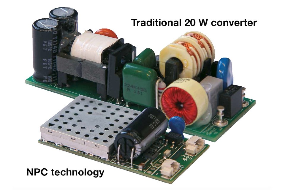
 Figure 4: Comparison of a 20 W driver with a switching frequency of 100 kHz and 30 MHz
 Figure 5: Efficiency curve for the 20 W driver operating at 30 MHz
Technical Advantages from VHF
Moving to higher frequencies has several advantages; where the main advantages are miniaturization, reliability/lifetime and dimming efficiency.
Miniaturization
Figure 1 illustrates that the passive energy storage elements constitutes most of the volume of an SMPS. As a rough average, these components constitute 95% of the volume and the active components together with resistors etc. the remaining 5%. Although the increase in switching frequency does not reflect one to one the size reduction, increasing the frequency 300 times from 100 kHz to 30 MHz will give a reduction of around 10 times. Hence, the overall SMPS will be reduced to approximately 15% of the original volume. This is illustrated in Figure 4 where a traditional 20 W LED driver operating at 100 kHz is compared to a 20 W LED driver operating at 30 MHz.
Reliability
A large share of LED system failures is caused by LED drivers; some claim a vast majority. This is, in most cases, due to the electrolytic capacitors as their lifetime is greatly reduced with temperature with the liquid inside them evaporating. The reduced need for capacitance at VHF eliminates (or significantly reduce) the need for electrolytic capacitors and consequently limits this failure cause.
Furthermore, decreased need for energy storage leads air core magnetics to be a feasible alternative to cored magnetics. The move to air core magnetics requires a significant jump in frequency, as less inductance per volume can be achieved without the core. If the frequency is increased into the VHF range, air core and PCB embedded magnetics become viable solutions, as the inductances needed at these frequencies can be made in a small physical size and the core losses avoided [7]. This does not only reduce the BOM significantly, but also improves the robustness and mechanical stability of the LED driver, as the magnetics components have the highest physical mass and are sensitive to high temperatures.
High dimming efficiency
Another strong benefit is increased dimming efficiency. Due to the very high switching frequency, it is possible to modulate the entire converter when dimming, without causing visible flicker. In this way, the converter is either on and operating under optimal conditions with the highest efficiency or off with will low losses. This enables a very flat efficiency curve. This can either be used to achieve higher dimming efficiency in a specific luminaire or to use a given driver across a wider set of luminaires while achieving high efficiency for all.
Figure 5 shows the dimming efficiency of the pictured 20 W indoor driver operating at 30 MHz.
VHF LED Drivers
The benefits of VHF power converters push the boundaries of power converters. The trade-offs done for traditional converters are, however, still relevant, as some parameters can still be improved further if the specifications for others are relaxed. The main optimization parameters are generally size, efficiency, reliability, cost and performance. A specific driver design can either use all the advantages of VHF to improve one or two parameters, or spread the improvement across all parameters as indicated in the spider web in Figure 6.
In this section two examples of VHF LED drivers will be presented. These drivers are both based on the class DE converter and primarily optimized for size (indoor) or reliability (outdoor).
Compact indoor driver
The 20 W driver shown in Figure 4 is optimized for an indoor luminaire with a slim profile, compact form factor, low cost and high dimming efficiency. The efficiency drops only 5% when dimming down to 10%.
The driver has a general build height of only 6 mm. The electrolytic capacitor is slightly higher, but could be reduced by splitting it into two thinner versions or making a cutout in the PCB. Another option is to replace the electrolytic capacitor with ceramic capacitors as shown in Figure 8. This increases the cost, but extends the lifespan and reduces the height.
Reliable outdoor driver
The requirements for outdoor lighting are different than for indoor lighting. While size is still relevant, lifespan and reliability are key parameters due to the cost of replacing a failed driver. The 60 W driver in Figure 10 is optimized for this application.
The driver is electrolytic free, which combined with a good electrical and thermal design ensures a lifespan beyond 120,000 hours at 75 degrees TC. Furthermore, it has built-in surge protection of 8 kV / 4 kA common mode and 10 kV / 5kA differential mode, again, to ensure high reliability and long lifespan. The driver is fully programmable and has all standard control interfaces. The driver has a slim profile of only 25 mm and the volume is approximately half of the closest solutions with traditional SMPSs.
 Figure 6: Trade-off parameters
 Figure 7: Compact 20 W LED driver without electrolytics
 Figure 8: Electrolytic free 60 W LED driver
Conclusions
LED drivers have become one of the main bottlenecks for LED lighting, both in terms of size and reliability. The technology behind VHF LED drivers provides fundamental advantages for LED lighting with smaller form factor, higher reliability and improved efficiency over the dimming curve. The design of a given driver can be adjusted to focus on benefits relevant for a given lighting application.
With the progress of traditional power supply solutions stagnating and the requirements for miniaturization due to the improvement of LEDs constantly increasing, new technologies and solutions are needed for the next generations of LED lighting. By combining circuits from the RF industry with the design methodology of power electronics, it is possible to design new VHF SMPS topologies with effectively no switching losses. Hereby, the need for passive energy storing elements is reduced, enabling removal of heavy and bulky magnetic components and temperature sensitive electrolytic capacitors.
References:
[1] M.D. Seeman. Gan devices in resonant llc converters: System-level considerations. Power Electronics Magazine, IEEE, 2(1):36–41, March 2015. ISSN 2329-9207. doi: 10.1109/MPEL.2014.2381456.
[2] J. Rivas. Radio Frequency dc-dc Power Conversion. PhD thesis, Massachusetts Institute of Technology, 2006.
[3] M. Madsen. Very High Frequency Switch-Mode Power Supplies – Miniaturization of Power Electronics. PhD thesis, Technical University of Denmark, 2015.
[4] D.J. Perreault, Jingying Hu, J.M. Rivas, Yehui Han, O. Leitermann, R.C.N. Pilawa-Podgurski, A. Sagneri, and C.R. Sullivan. Opportunities and challenges in very high frequency power conversion. In Applied Power Electronics Conference and Exposition, 2009. APEC 2009. Twenty-Fourth Annual IEEE, pages 1–14, Feb 2009. doi: 10.1109/APEC.2009.4802625.
[5] J.M. Rivas, D. Jackson, O. Leitermann, A.D. Sagneri, Yehui Han, and D.J. Perreault. Design considerations for very high frequency dc-dc converters. In Power Electronics Specialists Conference, 2006. PESC ’06. 37th IEEE, pages 1–11, June 2006. doi: 10.1109/ PESC.2006.1712114.
[6] M. Madsen, A. Knott, M. A.E. Andersen. Low Power Very High Frequency Switch-Mode Power Supply with 50 V Input and 5 V Output, IEEE Transactions on Power Electronics, December 2014, vol.29, no.12, pp.6569-6580.
[7] M. Madsen, A. Knott, M. A.E. Andersen, A. P. Mynster. Printed Circuit Board Embedded Inductors for Very High Frequency Switch-Mode Power Supplies, IEEE Energy Conversion Congress and Exhibition Asia DownUnder, Melbourne, Australia, June 2013. Conference Proceedings p1071-1078.
(c) Luger Research e.U. - 2017
