LED Failure Modes and Methods for Analysis
LED’s open the way to new applications and markets in various different fields with a broad spectrum of requirements. Beneath other beneficial characteristics, in general, LED’s provide a high reliability, and a lifetime of more than 50;000 hours can be reached. Poor workmanship in manufacturing and unfavorable operational conditions may reduce the reliability significantly. To avoid failures or to achieve fast resolutions of existing problems a good knowledge of the failure mechanisms and suitable analytical methods is required. Objective of this article is to provide an overview of state of the art techniques in LED-Failure analysis.

 and transmitted light (right) microscopy of a typical surface corrosion.")
 for different diode types.")

LEDs – Principal Function and Technologies
The LED-chip as the central element of the LED is a semiconductor that generates light in a PN-junction by electron p-hole recombination. The active zone is a complex structure of epitaxial layers. For different colors differential material-combinations are used: InAlGaP - red, InGaN - blue, GaAlAs - IR, AlGaN - UV. The material and the quality of the epitaxial layers essentially determine the efficiency factor of the generation of light.
The primary parameters for the function are current and temperature Tj within the active layer, influencing both the power consumption and the color, which significantly determine the lifetime as well.
LEDs are available on the market in different technologies. Essential and important criteria are a stable current path through bonding- solder- and glued connection, a sufficient cooling of the chip by a good thermal contact to the environment or appropriate heat sink, as well as a high extraction of light from the LED by optical elements and areas of reflection.
LEDs are encapsulated in general with transparent material like silicone or epoxy. For white LEDs phosphor is added to convert blue LED in a broadband, white appearing spectrum.
LED – Failure Modes
The defects occurring on LEDs can be related to different categories which are: the chip, as the central element and the internal and the external packaging. Due to the very different assembly technologies and types of constructions, as well as varying applications, an extended range of failure mechanisms can be observed.
Failure modes: Chip
During normal operation optical performance of LEDs gradually decreases during lifetime. In turn, this means a limitation in lifetime. Performance decrease is caused by growing defects in the epitaxy layers or on their boundaries, resulting in an increase of not radiating recombination and a decrease of optical efficiency. Usually a 30% or 50% decrease of optical performance is defined as defect while expected operation life is between 20,000 h and 100,000 h.
Ageing due to extension of defects is considerably dependent on junction temperature Tj and current. Therefore a sufficient control of these parameters is imperative for reaching expected lifetime.
Accelerated ageing, i.e. LED efficiency loss within a period lower than expected life, is caused by adverse factors like low quality of epitaxy layers as well as, often, an excess junction temperature due to insufficient heat dissipation. Furthermore, penetration of humidity or other contaminants, latent ESD (Electro Static Discharge) damage as well as an instable power supply can result in an accelerated degradation of epitaxy layers.
A catastrophic defect like a sudden failure can be caused by ESD or EOS (Electrical Over Stress) due to electrical overload resulting in a serious damage of the epitaxy layer.
Failure modes: LED internal construction
Interruptions in the current path respective the increase of electrical resistance have turned out to be frequent failure causes leading to reduced light emission, temporally instable function or even the entire failure. Delamination in the junctions between the chip and bond wire respective the chip and the substrate have also been detected. Since the interface area of the chip to substrate bond essentially influences heat dissipation, disruptions of the interface layer cause an increase of thermal resistance and chip temperature. Consequently, this leads to accelerated ageing of the LED.
In the LED production process are many failure sources to be considered. The soldering process has turned out to be especially critical because thermal overload can cause cracks, detachments or delaminations along the border areas due to the various expansion rates of the materials. Extensive qualification tests and stable quality control at the LED manufacturer as well a very good control of the solder process during PC assembly are basics for a long lifetime.
Transparent encapsulation materials like silicone or epoxy are not hermetically sealing and therefore do not protect against humidity or other damaging materials. Furthermore, mechanical stress, for instance while bending the pins of 2-pin-LEDs, or thermal stress like the soldering process, can cause cracks or detachments of the LED joint compound and allow penetration of contaminants down to the chip or metal contact. Under adverse conditions this will result in modifications of the epitaxy layers or in corrosions in the interfaces. Another effect would be the already described consequences due to detachment of the electrical joints or the performance degradation due to damaged reflecting surfaces.
Other typical mechanisms that lower the useful lifetime are the ageing of encapsulation materials influenced by UV-radiation, or the degradation of the phosphor of white LEDs, which is also responsible for a color change of white LEDs (known as yellowing). This effect is more intense than the regular ageing of a chip.
Failure modes: LED external assembly
By integration of LEDs in an external assembly, for instance in a PCB (Printed Circuit Board), more failure sources like malfunctions of electrical joints due to bad solder contacts must be considered.
Especially for high power LEDs, thermal contact and heat dissipation are very critical effects impacting degradation. The assembly should ensure and guarantee stable thermal contact during complete life.
Since humidity in LEDs, especially during the soldering process, may lead to the so called „Popcorn-Effect“, moisture-proof storage should be ensured.
In some applications the LEDs are covered by a protective lacquer or an external joint compound. Mechanical or thermal stress, as well as a reaction with outgassing materials can cause failures in the internal construction of an LED.
Methods for Analysis
LEDs present a broad range of failure modes which can be approached by using different methods of analysis. The objective of the failure analysis is to be able to allocate the observed failure pattern to a possible root cause and then show a way to avoid it. Because of the complexity, a failure analysis puts high requirements on technological know-how and the availability of methods for analysis.
Approach to find errors:
• Questions: In which environment was the LED/Module operated?For how long? Which driving mode was used?
• Measurements: Current/Voltage curves, intensity of light, wavelength/ color, radiation characteristics
• Non-destructive analysis: x-ray, light optical microscopy, scanning acoustic microscopy
• Destructive analysis: cross-sectioning, opening the package
• Physical analysis: FIB/REM, OBIRCH / Emission microscopy, EBIC, cathodoluminescence
In order to limit the extent of the examinations, it makes sense to develop an efficient strategy that will cover the most comprehensive amount of historical information at the beginning of the failure analysis.
Visual light microscopy inspection
The visual inspection provides information about the external construction, the external integrity of the LED package and accessible parts of the internal construction.
Opto - electric measurements
Essential opto-electric parameters are the optical power, the spectrum (color), and the current-voltage characteristics.
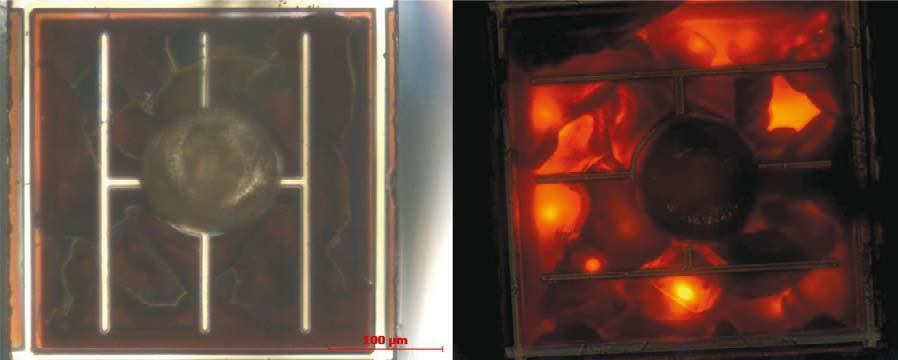
The radiation characteristics in the far- and the near field discover the inhomogenities of the light emitting area. Measurements of thermal resistance show problems in the thermal coupling.
Increased voltage in the forward direction points to a disturbance in the current path. Increased leakage current in reverse bias is a sign of a severe disorder in the epitaxy layers. This could be caused, for example, by ESD. The comparison of fine structures in the current/voltage curve between failed and working LEDs can help to differentiate between the various causes of errors.
See Figure 5 (see LpR magazine)
Other non-destructive procedures
Because LEDs are usually packed in plastic housings, detachment of the bond wire of the LED chip can be detected by using a x-ray microscope. The scanning acoustic microscopy is also suitable for identifying delamination on the interface.
See Figure 6 (see LpR magazine)
Destructive physical methods
To localise failures inside the LED, direct access to internal parts like the LED-chip or bond interfaces is required. Cross-sectioning or removing encapsulent materials by using chemical solvents are adequate treatment methods.
See Figure 7 (see LpR magazine)
The inside structures are then accessible for high definition optical or SEM microscopy, and failures at the interfaces can be detected. Material analysis with EDX can determine impurities in the case of corrosion effects and give an indication to possible causes.
See Figure 8 (see LpR magazine)
Failure analysis on chip level
To localize failures on chip level, methods are available that reveal defective areas on the chip, like dark spots or dark lines. Such methods are based on localized stimulation of light emission (cathodo luminescence) or current flow by pointing an external electro beam (EBIC) or laser beam (OBIC) onto the chip. Emission microscopy uses very sensitive detection of light created by leakage current.
Special methods like TEM (Transmission Electron Microscopy) and sample preparation using FIB (Fused Ion Beam) are required for the deeper analysis of failures in the epitaxy system layer. Evaluation of the results require the possibility for comparisons to the known error patterns and good models because the defective structures within the semiconductor are very dependent on technology used. Therefore these methods are very expensive and only used in special cases.
Summary
Basically, the reliability of LEDs is very high, but also dependent upon technology, construction technology and application requirements. The article shows the typical failure mechanisms, various types of analysis steps and with the results of this, ways to avoid future failures can be determined.
A good knowledge of typical failure modes will help to provide highly reliable LED products.
To gain this knowledge, it is necessary to adopt a systematic approach to isolate the failures, to use suitable procedures and methods for the analysis, to apply the correct way to generate and interpret error patterns of LEDs and, very importantly, to take prventive measures in order to avoid any possible problems.
