LED Lighting Requires New Approaches in Optics
LpR 67 Article, page 88: Even though LED technology has been established LEDs still need new approaches in electronics, thermal management or optics to make complete use of their advantages. Marek Škereň, Chief Technology Officer of IQ Structures, explains how new optical devices, with the trade name Nanoptiqs, based on principles of diffraction are applied to achieve improved performance of white light illumination systems. This unique solution is based on full control over the modulation of material and geometric properties of the optical elements at a nano-level. A combination of complex transmission diffractive elements, with specially designed systems of micro-reflectors (produced using an innovative mass-production technique) is also presented as a promising flexible building unit for the construction of new generation luminaires.
For a long period of time light from lighting systems was managed using conventional optical elements based on reflection or refraction. Large light sources required bulky optical systems, however, the beam shaping capabilities were rather low. It was almost impossible to achieve complicated light distribution curves (LDC), even for complex configurations of optical elements. An invention of LED based solutions for lighting applications introduced new degrees of freedom to the design of luminaires. The most important parameter from this point of view is the size of an LED chip, which is significantly smaller than the typical dimensions of conventional light sources. Generally, a small light-emitting volume enables miniaturization of optics and complete luminaires. However, the highest potential follows from a significant increase of spatial coherence of the emitted light. New approaches based on diffraction of light from micro and nano-structured materials can now be used for extended shaping of light distribution curves. Application of diffractive elements dramatically increases flexibility of the beam shaping process and enables precise illumination of areas with complicated shapes and requirements with a spatial distribution of energy. Such capability results are not only a significant improvement in the quality of illumination, but it can also lead to an important increase in overall efficiency of illumination systems and reduction of energy consumption. Moreover, in most cases the systems based on diffractive elements are lightweight, convenient for mass production and have lower environmental impact following from their production and disposal. The presented approach opens new interesting possibilities also for visual design of future light fixtures. The designers benefit from significantly higher flexibility of shapes of optical components. The complexity of the optical function is not any more closely connected with the complex geometry of the optical elements. Thus, smooth designs with simple geometric shapes can be used in combination with the sophisticated optical performance of the luminaire. Also, the geometric dimensions of light fixtures are positively influenced, extremely thin or narrow bodies can be constructed (Figure 1).
 Figure 1: The picture of a luminaire based on the new technology approach demonstrates the wall-washing effect of a surface-emitting, ultra-thin, low-glare luminaire with visually homogeneous luminous surface
Physical Principles and Design Approaches
Application of principles of diffraction for managing light from illumination systems requires several important issues to be addressed. The most critical one is the strong dispersive behavior of diffractive structures under polychromatic illumination. The diffractive dispersion is naturally much stronger than the dispersion of refractive systems. There are several approaches to the suppression of coloring effects; some with stronger emphasis on color properties and others oriented more on diffraction efficiency of the elements. The new solution is based on sophisticated calculation of three-dimensional nano-structured elements with high resolution. The design and optimization is performed by polychromatic light using in-house developed numerical tools. Due to the high amount of processed data and large number of parameters the calculation is extremely computationally intensive. On the other hand, it is possible to tune the behavior of the system for polychromatic light exactly according to the needs of a particular application. Manufacturing of the designed micro/nano-structures is also highly demanding due to the complex nature and modulation of the material properties. Especially important is the orientation of micro/nano-structures with such a geometry, which already fully suppresses the unwanted dispersion, but, simultaneously, it is still applicable for effective mass-replication processes. Similar structures are still used more and more, not only in lighting applications, but also in other optical systems. However, these microstructures are usually one-dimensional and the shaping functionality is rather limited. To achieve full flexibility in operation it is essential to use full threedimensional micro/nano-structures. Such elements are still, in general, highly demanding from a point of view of design and mastering processes.
 Figures 2a&b: Schematic illustration of the luminaire from figure 1 (a). The active part of the system, as thin as 6 mm, consists of a combination of circuit board with LED chips, specially designed microreflectors, and nanooptical element (b)
Higher complexity of the micro/ nano-structure induces volume behavior of the diffractive element also for relief-type structures. Thus more rigorous modeling approaches must be used to simulate the interaction of light with optical elements instead of simple ray-tracing techniques. The numerical tools have been developed to simulate light interaction with structured matter in a fully vectorial form. These tools in combination with commonly available ray-tracing software packages are integrated within the design and simulation of the systems. The micro/nano-structure is calculated point-by-point with resolution better than 100 nm, very often reaching values down to 10 nm. Thus, the design process is extremely computationally intensive and requires state-of-the art computer hardware.
Complex Hybrid Optical Systems
Although the diffractive structures are very flexible and capable of sophisticated operation, it is often difficult to achieve required functionality just by using a simple micro/nano-structure. In such cases, more complex nano-optical elements can be used with general three-dimensional modulation of material parameters. The described complexity has significant impact on the design and modeling processes, thus special tools have been developed to cover such needs.
To achieve maximum flexibility of the systems, it is necessary to handle one more important issue connected with the widespread application of wide-angled LED chips with Lambertian emission. To collect as much light as possible from the chip, a type of reflection barrier or micro-reflector could be used. The complete assembly can be constructed according to the drawing displayed in figure 2. The system of micro-reflectors performs pre-processing of the light incident in the transmission optical element. The reflected light, together with the direct beam from the LED source, is further managed by a transmission optical micro/nano-structured element. Because of high demands on spatial coherence of light at the plane of the optical element, the whole system must be designed, simulated, and optimized within a single loop within the same design environment. The developed design packages take into account all of these aspects.
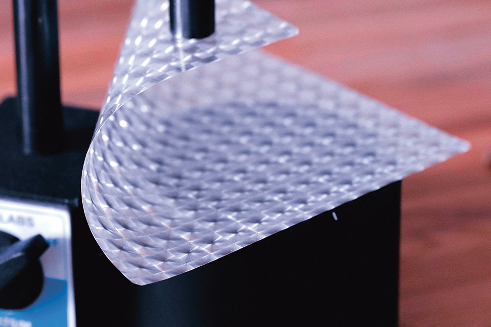
 Figure 3: Only an optical foil like this, based on the presented new technology, allows the luminaire design and light distribution shown in figures 1&2
When multiple LED chips are used on a single circuit board, the described combination of reflectors and sophisticated transmission elements can serve as a building unit for larger luminaries. Particular functionality (LDC) of each such unit can be tuned separately from the neighboring cells without visible changes to visual appearance of the unit. The change itself can be realized through replacing only some of the components in the optical system. Such a level of flexibility is extremely important from a commercial point of view as the chance to tune the LDC without replacing the complete optical system is highly interesting in many applications.
Manufacturing, Mass-Replication and Commercial Application
Apart from the improved functionality, this approach is distinguished by a significant increase in efficiency of mass production. The micro/nanostructured reliefs can be effectively mass-replicated using various types of embossing processes. Very often, a roll-to-roll technology can be used with large widths and high throughputs. On the other hand, mastering of the tool for massreplication is a tricky task with high demands on precision and elementary feature size. Manufacturing of three-dimensional optical nano-structures requires application of state-of-the-art mastering techniques with extreme spatial resolution.
 Figures 4a&b: Both figures demonstrate the advantage in size for the new optical approach compared to a reflector (a) in diameter, and to a conventional lens (b) in thickness
In many cases, micro-reflectors represent important parts of the solutions, which improve efficiency, and overall performance of the system. On the other hand, application of precise miniaturized systems of reflectors based on extruded aluminum or injectionmolded plastics are questionable because of high costs, low throughputs or limited precision of shapes. Therefore, a completely new technology has been developed, which is based on the shaping of thin plates from a wide variety of plastic materials. The invented technique features high throughputs, high efficiency of manufacturing process and excellent fidelity of created shapes. Simultaneously, thin plastic carrier material ensures low weight and high resistance against environmental influences. Altogether, the described properties promise excellent applicability of the micro-reflectors in a wide variety of applications.
An example of the luminaire based on the new solution is presented in figures 1 & 2. The photo of the luminaire of figure 1 demonstrates the wall-washing effect of a surface-emitting, ultra-thin, low-glare luminaire with visually homogeneous luminous surface. Such a performance cannot be virtually achieved using conventional manufactured optics components.
Conclusion
The presented approach to design and manufacturing of optical systems for lighting applications is distinguished by a significantly improved optical performance and completely new parameters for manufacturing processes. It was demonstrated that new complex functionalities could be achieved without decreasing the efficiency of manufacturing. On the contrary, in most cases the mass-production of these components is more effective and robust when compared to manufacturing of conventional optical systems. Although mastering of the production tools is often demanding and can require the application of the latest state-of-the-art technologies, the mass-replication step is very efficient. Altogether, the proposed solution represents a promising direction, not only in general lighting applications, but also in the fields of light management for automotive industry, optical sensors, traffic and pedestrian lights, and many more.
