Looking for the Best Thermal Solution for CSP Module Designs
Chip Scale Package (CSP) LED technology is not new but while it has been used for a while in TV backlighting applications, it is relatively new to lighting applications. In many respect CSPs are a new world for lighting module manufacturers as they are smaller, usually don’t have any ESD protection, have different light distribution, and, last but not least, have a smaller heat dissipation area. The latter asks for re-thinking the traditional thermal design for modules. Dr. Giles Humpston, Applications Engineer at Cambridge Nanotherm, explains in detail why CSP LEDs present a significant thermal challenge for module designers and outlines some fundamentals in calculating the thermal flow required to keep CSP LEDs cool.
CSP LEDs, the latest incarnation of flip-chip LEDs, began their life in backlighting for TVs. In these applications low and mid-power LEDs were used without any problems. As the market moves inexorably towards general lighting, the power rating of CSPs is creeping up. CSPs for general lighting fall into the ‘high-power’ category (over 1 W) and with devices rated up to 3 W currently available, this is causing problems.
The term ‘chip scale package’ is defined by the package being no more than 20% larger than the chip itself (the next step is wafer level packaging where the packaging is the same size as the chip). To achieve this, LED manufacturers strip out as many of the superfluous elements as possible. Take a standard high-power packaged LED and remove the ceramic submount and the wire bonds, directly metallize the P and N contacts and coat with a phosphor and you have a CSP LED. This method is great for LED manufacturers as it reduces both the material and manufacturing costs. It also results in a very small (often 1x1 mm) packaged LED that can be closely packed onto PCB modules, helping to create smaller, brighter and cheaper luminaires.
As a result of these benefits the CSP market is enjoying strong growth. Industry analyst Yole Développement estimates that CSPs will make up 34% of the high-power LED market by 2020.
Why CSPs Present Such a Thermal Challenge
However, CSPs aren’t without their challenges. The small dimensions can present handling problems for pick-and-place machines. The absence of a lens means careful consideration needs be given to beam management. But most immediate is the thermal challenge posed by the move towards ever higher-powered CSPs.
CSPs are designed to be soldered directly onto a PCB using their metallized P and N contacts. This reduces the thermal resistance between the LED die and the PCB which, viewed from one perspective, is a positive thing. However, the absence of the ceramic submount that acts as a heat spreader between the die and the board in a traditional packaged LED means heat transfers from the die to the PCB as an intense point heat source. The thermal management challenge has, effectively, been shifted from “Level One” (the LED die packaging level) to “Level Two” (the module level). This means that module and luminaire designers have to be extremely careful to ensure CSP LEDs are provided with adequate cooling. To meet these demands Metal Clad PCBs (MCPCBs) with aluminium or copper bases are used.
To illustrate this, let us consider an example of a wire bond LED that measures 1x1 mm attached to a standard ‘Level One’ submount, made of aluminium nitride and measuring 3.5 mm on a side and 0.635 mm thick. In this instance the heat source is 1 mm2 and assuming the thermal conductivity of the aluminium nitride is isotropic, a simple thermal model reveals the heat will spread to cover an area of approximately 5 mm2. Obviously, most of the heat remains concentrated in the central area but even so, the effect of the submount is to decrease considerably the heat flux density before it reaches the module MCPCB. With a CSP LED, the reverse applies. Again, taking a 1x1 mm device, the solder lands must be smaller than this and might only measure 0.3x0.8 mm each. This reduces the initial area available for heat transport by roughly half so less spreading has occurred by the time it reaches the cold side of the submount. This equates to a 2-fold difference in cooling ability between the CSP LED and a wire bond LED on a submount.
The price of failing to remove this heat effectively can be a reduced lifespan, poor light quality, color fluctuation and ultimately catastrophic failure of the LED.
In the absence of a submount, for CSP LEDs it is solely down to the MCPCB to conduct the heat effectively enough to keep the LED junction temperature within the manufacturer’s recommended limits. This challenge becomes even harder as CSP LED dimensions shrink, power ratings increase and the module designer packs more and more CSPs into ever denser arrays – the MCPCB now really needs to work for its money.
To better understand the scale of this issue it is necessary to break this down. to a heat sink, illustrating the spreading that occurs, effectively decreasing the thermal resistance of the path") Figure 1: Thermal model of the heat flux emanating from a 1x1 mm CSP LED through a 0.635 mm AlN submount (170 W/mK) to a heat sink, illustrating the spreading that occurs, effectively decreasing the thermal resistance of the path
Figure 1: Thermal model of the heat flux emanating from a 1x1 mm CSP LED through a 0.635 mm AlN submount (170 W/mK) to a heat sink, illustrating the spreading that occurs, effectively decreasing the thermal resistance of the path
 Figure 2: Radial heat spreading from a point source of heat in a copper disk, having dimensions representing a generous copper area of wiring trace on a MCPCB
 Figure 3: Simplified simulation of a CSP LED on a MCPCB illustrating that a 60 um copper wiring trace is unable is to spread the heat laterally any significant distance. The close similarity of heat flow with figure 1 is to be expected when the substrate is a high performance MCPCB having an aggregate thermal conductivity in excess of 150 W/mK
Considerations on Calculations
When calculating the thermal flow in CSP designs, the primacy of axial conduction is important:
First, it’s worth considering that in most CSP LED board designs, efficiency of axial thermal conduction tends to play a more important role than that of lateral thermal conduction. In this context, axial thermal conduction is z-axis, i.e. through the thickness of the MCPCB while lateral or radial thermal conduction is in-plane in the x/y-axis and occurs predominantly in the copper wiring trace of the MCPCB.
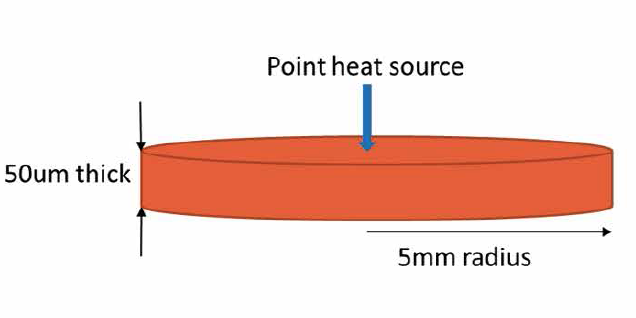
To illustrate this, consider a standard CSP LED soldered to a copper circuit layer, of around 50 μm thick and 35 mm diameter, which in turn sits on a dielectric, and then an aluminium heat spreader. Depending on the grade of the board the thermal conductivity of the dielectric will typically range from around 3 – 10 W/mK and between 10 and 50 μm in thickness. This means the axial thermal impedance will range between 0.16 and 0.01°C∙cm2/W. That is, for a slab of dielectric measuring 10 mm on a side, every watt of heat flowing will not pass through instantly but result in the calculated temperature difference (0.16 - 0.01°C) between the two faces.
The next step is to examine the radial thermal resistance of the copper disc. Copper is an excellent conductor of heat, with a thermal conductivity of almost 400 W/mK. But at only 50 μm thick, which is half the thickness of a human hair, its ability to transport heat along its length is severely restricted. Taking a bar of copper 1 mm wide by 50 μm thick by 5 mm long the thermal resistance end-to end is over 250°C/W. Clearly this is massive compared to the axial thermal resistance so when the copper disk is attached to a dielectric layer with very low thermal resistance, most of the heat will promptly disappear through the dielectric and down to the heat sink and none will get as far as the edge of the copper area.
This is demonstrated by expanding the previous simulation to include a 35 um thick layer of copper covering the whole 3.5x3.5 mm area, but keeping the hot CSP LED the same dimensions. The model shows some heat spreading taking place in the copper but the extent is limited to a 15% increase in area at the heat sink.
In practice for optimum cooling of CSP LEDs it is necessary to balance the axial and radial conductivities. If the copper area is overly reduced, too much reliance is placed on axial conduction so the thermal resistance goes up. This means that close packing of CSP LEDs can result in thermal imbalance over the array area. Conversely, making the copper area excessively large has little benefit because of its high in-plane thermal resistance that prevents the heat spreading any significant distance.
Often it is assumed that specifying a thick layer of copper on a MCPCB will spread the heat far and wide, reducing the flux density and making it easy to remove the heat by conduction through a dielectric with mediocre thermal resistance. While this is true to a certain extent, only the very best MCPCBs have sufficiently low thermal resistance to accommodate high power CSP LEDs. With these products, increasing the thickness of the copper does not change the optimum copper area (of around 3.5 mm diameter) because the in-plane thermal conduction of even a 105 um (3oz) thick plane of copper on a decent quality MCPCB is still low relative to z-axis conductivity of the dielectric. There is also the constraint that the copper tracks underneath a CSP LED are required to possess a gap of around 200um and this becomes progressively more difficult as the thickness of the copper increases.
In any thermal analysis of LED structures, it must be remembered that the thermal path between an LED and a heat sink is not a solid lump of homogeneous material. Usually it comprises a complex stack of materials, such as the LED package, solder joint, circuit board, thermal interface material, heat spreader and many more. Each of these structures will have radically different dimensions, thermal conductivities and specific heat capacities, with various interface resistances between all the different layers. Of these, interface resistance is often the most critical and one of the hardest to model. The thermal resistance of a single interface can dwarf the thermal properties of the other materials in the structure and throw calculations of performance to the wind. The best technical solutions seek to minimize interface resistance between elements in the board, the most assured method of doing this being by elimination from the structure. Coatings and other layered constructions are particularly vulnerable to high interface resistance and the possibility it will change over time. While homogeneous materials are best, where an assembly of different materials is necessary, the most robust and reliable approach is to achieve bonding at the atomic level between materials. Only a limited range of coating and deposition processes function on this premise.
About the Ideal Profile of an MCPCB Solution for CSP LEDs
So, to reiterate, high axial conduction through the MCPCB is key to a successful CSP design. When the axial conduction is high it negates the heat spreading benefits usually found by using a thick copper wiring trace. To effectively manage the point heat flux generated by CSPs requires a different approach to the MCPCB itself.
Based on the observations of axial primacy outlined above we know that the MCPCB needs to minimize the thickness of its weakest link – the dielectric layer. Thermal resistance is thickness divided by thermal conductivity. Thermal conductivity is intrinsic to the material selected for the dielectric so the only variable available is thickness. Diamond is perfect for this application but too expensive. The dielectric cannot be too thin as it needs to maintain acceptable electrical isolation to ensure the MCPCB is compliant with relevant regulation. The dielectric layer must also be robust enough to withstand the manufacturing process and durable enough to last active service. And finally, the MCPCB stack needs to minimize the interface resistance between the various materials to maximize the composite thermal conductivity.
 Figure 4: Graph demonstrating that for a MCPCB with adequately low thermal resistance to accommodate CSP LEDs, the copper weight has negligible impact on performance
Alternative Solutions to MCPCB for CSP LEDs
Almost all MCPCBs follow the same basic format in terms of their construction: They are manufactured from a sheet of metal (usually aluminum, sometimes copper) covered with a thin (30+ μm ) layer of copper for the wiring trace. This copper sheet is attached (and electrically isolated from the metal base) by a dielectric layer of epoxy resin filled with particles of thermally conductive ceramic to increase thermal performance. However, there is an upper limit to how much of the thermally conductive ceramic can be added. Overload the epoxy with ceramic and the dielectric layer becomes friable and the adhesion to the metal substrate and copper wiring trace will be poor. Not good for a product that needs to be sturdy enough to last several decades (50,000 hours) of active service.
Whilst there are always new developments in these thermally conductive dielectrics there is always a trade-off between performance and durability. At the moment this limits the performance of MCPCBs to a composite thermal conductivity of well under 100 W/mK.
This thermal performance is perfectly acceptable for a majority of LED module designs, but when it comes to CSP modules, particularly for power dense designs, they simply do not offer the required performance. Historically there was only one option available to manufacturers when the thermal performance of MCPCBs fell short of requirements, and that was to move to a wholly ceramic substrate such as aluminium nitride; a material with exceptionally high thermal conductive and an exceptionally high price tag to match.
By taking the best elements of both ceramic and metal PCBs, nanoceramic utilizes the primacy of axial conduction and a low interface resistance to optimum effect.
How Nanoceramic as Solution for MCPCBs Works
A patented electro-chemical oxidation (ECO) process converts the surface of a sheet of aluminum to a layer of alumina (Al2O₃) that is just tens of microns thick. Whilst alumina is not a particularly efficient thermal conductor (around 7.3 W/mK for the alumina created by the ECO process), the thinness of the layer means heat has an extremely short journey to make before hitting the aluminum base.
An interesting side effect of the ECO conversion is that the alumina layer is atomically bonded to the aluminum base. This has a significant impact on the interface resistance between the two materials helping to reduce the overall thermal resistance of the stack. The robustness is also impressive and it is impossible to mechanically cleave the nanoceramic off the aluminum from which it was formed.
This combination of a very thin dielectric layer with relatively high thermal conductivity, atomically bonded to the aluminum base, gives a MCPCB containing nanoceramic with laminated copper an exceptional overall thermal conductivity of around 115 W/mK (the copper wiring trace are attached to the nanoceramic with a 3-5 μm epoxy layer). This makes this product ideally suited to the demands of CSP applications.
Conclusions
As designers continue to explore what is possible with CSP LEDs they are regularly finding their designs are outside of the capabilities of standard MCPCB technology. This thermal limit is putting a barrier in the way of innovation and a new technology is needed to fill the gap between traditional MCPCBs and expensive aluminum nitride ceramics. Nanoceramic is one material able to fill this niche. By offering a thermal performance that is tailored to the intense point flux requirements of CSP LEDs along with drop-in manufacturability, an MCPCB with nanoceramic dielectric bridges the gap between traditional MCPCBs and ceramics, enabling CSP LED designers to push the limits – creating smaller, brighter and more cost-effective light sources.
