Mastering Thermal Issues in LED PCB Design & Laminate Selection by Ventec Europe
LED applications are not the only applications that are driving the need for thermal issues to be considered and mastered in PCB design, but they are certainly amongst the most challenging. Designing LED PCBs requires many considerations and key are those that arise from multiple heat sources in close proximity. Martin Cotton, Director OEM Technology of Ventec Europe describes the process and criteria used when designing PCBs (Printed Circuit Boards) for use in LED applications using thermally conductive IMS (Insulated Metal Substrates). He goes into technical detail with charts and diagrams that explain everything the designer would need to consider when selecting a laminate and commencing a design.
A PCB design for LED lighting products belongs to the most challenging tasks, a proper process and criteria is very helpful when designing PCBs (Printed Circuit Boards) for use in these applications using thermally conductive IMS (Insulated Metal Substrates). Therefore, the requirements for thermal management and the various issues that form the development of design rules and build structure for the Printed Circuit Board will be outlined in the article. Furthermore, the manufacturers specification and those provided by the laminate vendor are considered to create workable design rules that include coin cavity and adjacency dimensions. It looks at options for thermally conductive laminates; glass reinforced thermally conductive prepregs, thermally conductive dielectrics and IMS (Insulated Metal Substrates) materials.
A focus is on the make-up of these IMS in the form of copper-laminate-aluminum or copper-laminate-copper, considering the various characteristics, benefits and the thermal conductivity and impedance of each option.
Introduction
Various methods have been considered, tested and used in the dissipation of heat from the PCB and from the devices on the PCB. The most obvious and perhaps the traditional solution is the heatsink - a piece of metal with a large surface area provide space for the heat to flow into the air having been swiftly and efficiently removed by conduction from the device or heat source. As well as device mounted heatsinks, PCB mounted heatsinks are often used to connect the heat source to as large an area of conductive material as possible, often covering the entire unoccupied surface area of the PCB.
 Figure 1: The images below show the thermal impact of LEDs and of other devices such as processors
More recently, laminate technology has come to the fore and the use of in-PCB heatsinks, such as coins, has become more prominent with large areas of copper being used as “heatdumps” to deposit and dissipate thermal energy. These are sometimes within a space milled into the PCB surface, but can even be on inner layers and sometimes on multiple layers connected by through-hole plating. In simple terms a coin is a thermal heatsink within a PCB.
It is tempting to take a very industrial approach to heatsinking, placing a heatsink as large as you can fit on the offending device. This is a somewhat unscientific approach and may result in shifting the problem elsewhere as well as being more costly than the designed and calculated solution.
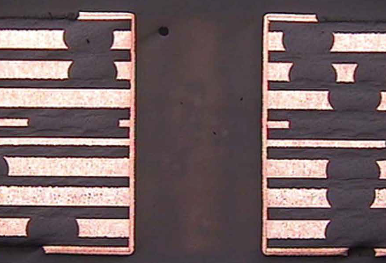
 Figure 2: Various methods are used during the PCB fabrication process to provide heat dissipation via areas of copper called coins
Designing with Coins
The coin cavity cross section design is critical and minimum clearance as well as maximum and minimum tolerances are generically required.
As can be seen in figure 3, the size of the coins is critical along with its proximity to other PCB features such as through-holes and inner layer traces and other components on the PCB. These dimensions will differ when the board is conventional PTH (Plated Through- Hole) as compared to boards that use micro-via technology.
 Figure 3: Coin dimensions & tolerances
For this reason early consideration of the heat dissipation requirements are essential. Creating design rules that apply to the coin cavity should be done at the same stage as the specification of the laminate and the other design rules around layer count, track and space, etc.
Design rules are required and start with what a designer wishes to produce. They are conjoint feedback from manufacturing and design on what minimum or maximum dimensions apply, plus the tolerances associated with those manufacturing processes. The designer will be pulling together data from a broad team of participants starting with the hardware designer who should provide detail on the devices used and their thermal characteristics. This data, combined with that from the PCB manufacturer and the laminate supplier, will ensure the correct choice of materials is made and the process tolerances are applied along with the dimensional demands from the thermal requirements and challenges. These dimensions and tolerances are then applied to any drawings required by manufacturing to produce the product and shared and approved by the various stakeholders to ensure all parties have an input into the most desirable, effective and economic choice of heat dissipation, laminate selection and fabrication methodology.
 Table 1: A typical set of coin design rules and associate dimensions
Design rules are created not only for what we are currently able to produce, but also to push the boundaries of what we might need to build in the future. This drives the technology roadmaps of the parties involved, largely the fabricator and laminate manufacturer.
Development programs come out from these “design” requirements, and they should. As laminate producers we want to make products that meet and surpass current and future demand. We should avoiding developing technology because we can, and focus on developing what we, our customers, and our customers’ customers need.
Consideration needs to be given to the laminate thickness when specifying the minimum distance between coins. Coins can be of varying thicknesses and can also be on the same or the opposite sides of the PCB. These all have different thermal impacts as well as dielectric considerations, while some strategies may impact on potential delamination. The PCB is a three dimensional component and the impact in the X, Y & Z axis needs to be considered in detail.
Each coin cannot be treated in isolation. They all impact upon each other and proximity is critical, as is the differing heat load of each coin. High load coins will need to be separated from each other, sometimes by laminate and other times by low load coins.
 Figure 4: Heatsinks could become connector routes as well as thermal coins
Replacing Coins with “Local” Heatsinks Using IMS Materials
Thermally Conductive IMS PCBs offer various solutions, with various component parts. These include:
• Thermally conductive laminates
• Glass reinforced (VT-4Ax) thermally conductive prepregs, unsupported (VT-4Bx) thermally conductive dielectrics
• Insulated metal substrate (IMS) materials
As an alternative or replacement to coins, this provides the ability to manufacture or fabricate local heatsinks on the PCB.
Coining and local heatsinks are very specific solutions, aimed at prime components and focused at a component level. IMS is broader and is less focused, but perhaps needs a better and more detailed design strategy, particularly if you want to move it away from a specific PCB by PCB solution or technology level to a more generic solution. Certainly the LED industry is asking a lot of questions and making great demands for better thermal management. The PCB fabrication industry and the laminate producers need to work in concert with the PCB and hardware design community to ensure they specify and create the best solutions.


Figure 5: Examples of data sheets
As part of the design process it is essential to create a test process that considers all the elements in creating a workable solution. It is easy to study the data sheets and compare materials that way, but each project needs to be carefully considered, as many factors impact upon the final selection of material.
Many experienced designers and engineers will say that whilst the data sheet is the ideal starting point, it does not provide the whole answer. This is not because vendors set out to produce misleading data, it is because data sheets are based on tests performed by the vendor in a certain environment and in certain circumstances that will inevitably be different from your derived data.
Studying the data sheets requires the consideration of many elements, not least the material build. Also important to consider are the thermal conductivity of the various materials as well as the thickness of the copper, the dielectric and the aluminum and aluminum alloy.
Reaching out and building a close relationship with the technical team at the laminate vendor will be very valuable at this point. They should be able to walk you through the selection criteria for their materials. Some vendors will have elements of design expertise within their team, but some may not. Working with a vendor with a sound understanding of the design principals is very important if you are to use the right material rather than one which will work because it is vastly over-specified for the task at hand and hence too expensive.
When doing the thermal calculation it is also essential to consider the thermal configuration and not just the resistance or conductivity, but also the thermal impedance, which many consider a more consistent and accurate measurement.
One influencing factor is environmental. Where will the PCB operate? Will it be potted? Will the flow of air around it change in different applications and will it deteriorate over time? A key factor in selection is reliability, but just building in the maximum reliability and maximum heat dissipation is an expensive and lazy solution, which will doubtless be costly.
Another environmental factor is the surrounding product and the impact that it has on thermal management. If the product dissipates heat in a way that negatively impacts on other products, that will automatically create and problem. Conversely other products or devices in close proximity will impact the thermal performance of the design.
Also important in material selection are mechanical properties and mechanical stresses that the product may be under in the field.
Manufacturing processes have to be considered and the fabricator and assembler will each have their input into the best solution. In this process you will also need to consider compliance to agency or customer approvals.
 Figure 6: Thermal system configuration
Conclusion
At the end of the day the solution needs to suit the product and be cost effective, not belt and braces because we don’t understand the parameters at play. Short cuts will result in one of two outcomes: A product that isn’t fit for purpose; or a product that is so over-engineered that it fails to be a cost effective solution.
