MOCVD Platform for Cost-Effective Production of GaN-based HB LEDs
GaN-based blue and ultraviolet light emitting diodes (LEDs) are steadily becoming more widely used in solid-state lighting (SSL) applications [1-3]. Enabling dramatic energy savings when compared to contemporary incandescent bulbs and fluorescent lamps, these high-brightness LEDs (HB-LEDs) have a market potential in the billions of dollars. Yole Development estimates that by 2017, the market for LEDs will be approximately $75 billion [4, 5]. Shiping Guo, the Senior Technology Director of Advanced Micro-Fabrication Equipment Inc. presents a new approach to support this goal with a cost effective MOCVD solution for HB-GaN LED manufacturing.
The greatest barrier to accelerating the widespread adoption of HB-LEDs is cost-per-watt parity. Although decreasing LED bulb prices, coupled with concerns about reducing energy consumption, are helping to position LEDs as the de-facto alternative to traditional incandescent and fluorescent (FL) lamps, their commoditization poses a challenge for manufacturers. According to a Yole Developement report [4], the price of today’s LED bulbs is approximately ten times higher than that of incandescent bulbs and approximately three times higher than that of FL lamps.
While MOCVD has shown to be the superior technique for growing III-nitride materials for optoelectronic and electronic devices, and producing the highest quality/best-performing devices, it is an expensive process. Almost a quarter (21 percent) of total LED manufacturing costs derive from the epitaxial growth process alone, with MOCVD reactor depreciation accounting for the lion’s share of those process costs. Clearly, the key to accelerating HB-LED adoption lies in effectively reducing manufacturing costs to ensure the competitive pricing and acceptable margins needed for LED manufacturers to succeed.
To address these economic imperatives, it will be essential for future-generation MOCVD tools to improve process efficiencies. This means demonstrating superior process performance and high-quality manufacturing capability. Excellent tool uptime is a must, as well as high throughput, good reproducibility and high yield.
Tests with a new MOCVD reactor show promising results to provide these performance characteristics and capabilities. Quality data from single layers, as well as LED wafers grown on the new platform, brightness results and data from a min-marathon test that demonstrates excellent growth reproducibility and tool function stability prove the performance of this now MOCVD platform – the so called Prismo™ D-Blue. FIgure 1: The four reactors of the new MOCVD platform
Design and Experimental Details
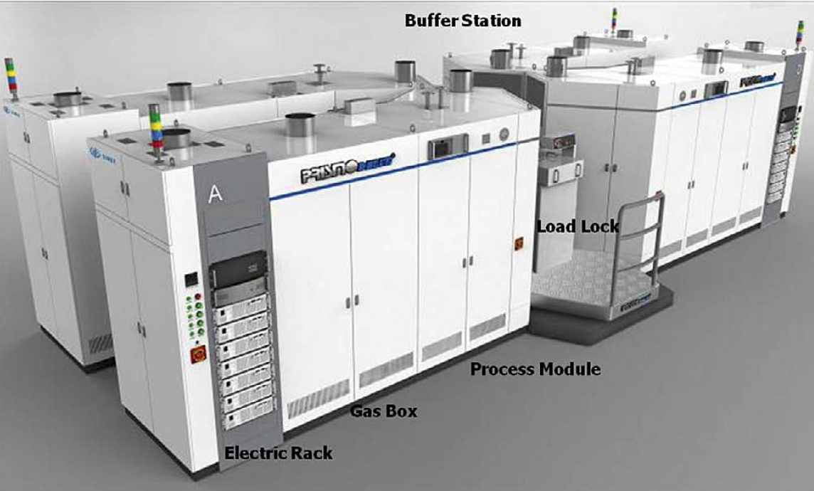
The new patented MOCVD platform architecture can accommodate up to four reactors, as shown in figure 1. Each reactor consists of a process module, gas box and electric rack. The load lock and buffer station are shared by all reactors. Each reactor can be controlled independently, enabling the use of various (49/54 x 2”, 14 X 100 mm, 5/6 x150 mm or 3 x 200 mm) susceptor patterns—a design that enables exceptional manufacturing flexibility. The platform architecture controls critical gas precursor dynamics through a unique combination of uniform gas laminar flow and high-speed susceptor rotation to ensure the formation of a uniform boundary layer. This enables high-volume manufacturing of the GaN, InGaN and AlGaN thin layers required for high-brightness LED structures. The platform is fully automated, with precise parameter control and an ultra-compact design.
All GaN-based epilayers and LED structures were grown on either flat sapphire substrates or patterned sapphire substrates (PSS). Trimethylgallium (TMGa), triethylgallium (TEGa), trimethylaluminum (TMAl) and trimethylindium (TMIn) were used for group III precursors and ammonia (NH3) was used for group V nitrogen. Silane and bis(cyclopentadienyl) magnesium (Cp2Mg) were used for n-type and p-type dopants. The GaN LED structures consisted of a low temperature GaN nucleation layer, an unintentionally doped GaN buffer layer (including a 3-D roughing layer and a 2-D recovering layer), a Si doped n-type GaN layer, InGaN/GaN strain engineering layers, InGaN/GaN MQWs, an Mg-doped p-AlGaN electron blocking layer, an Mg-doped p-GaN layer and a p+-GaN layer.
A variety of tools were used to establish experimental results. A Bruker D8 XRD system determined crystalline quality and aluminum content, while a Lehighton Eddy current system measured sheet resistance (Rsh). An HL5500 system was used to perform the Hall test, and a Bruker Dimension Edge atomic force microscopy (AFM) system was used to measure surface morphology. An Accent RPM2000 system measured total layer thickness and room temperature (RT) photoluminescence (PL) emission wavelength.
 Figure 2: The SIMS spectra of GaN based LED structures
Results and Discussion
Control of background doping levels is critical for MOCVD performance and epitaxial growth process development. Figure 2 shows SIMS spectra of a GaN-based LED structure grown on a 2” sapphire substrate. Very low background doping levels were observed for O, C and H in the n-GaN layer. Optimizing the growth conditions for the 3-D roughing layer and 2-D recovering layer enabled high crystalline quality GaN epilayer growth on both 2” and 4” sapphire substrates with a typical XRD FWHM of <250 arcsec for (002) reflection and of <300 arcsec for (102) reflection. Many XRD satellite peaks with clear interference fringes can be observed from InGaN/GaN MQW samples (as shown in Figure 3), indicating the high crystalline quality and sharp InGaN/GaN interfaces. The Hall test shows that the electron concentration in the various Si-doped n-type GaN layers is almost linearly dependent on the silane flow. A high electron carrier concentration of up to 1x1019cm-3 was achieved with an activation efficiency of >99 percent. Lehighton measurements of n-GaN wafers from different rings showed excellent ring-to-ring uniformity. Sheet resistance uniformity for all wafers from different rings was <1 percent. SIMS measurements demonstrated a maximum Mg doping concentration of approximately 2x1020 cm-3 in the p-GaN layer with a hole carrier concentration as high as 5x1017cm-3. These results were equivalent to or better than those from GaN layers grown in reactors from comparable tools available on the market [6, 7].
 Figure 3: Typical XRD satellite peaks with clear interference fringes from the InGaN/GaN MQW sample
Figure 4 shows total layer thickness and RT PL emission wavelength mapping of full susceptor (49x2”) loaded InGaN/GaN MQWs grown on a 2in sapphire substrate. The average thickness is approximately 6 μm with an average within-wafer uniformity of 1.0 percent and wafer-to-wafer uniformity of 0.4 percent. The average PL emission wavelength is 454 nm with excellent within-wafer uniformity of 0.3 percent and wafer-to-wafer uniformity of 0.3 percent (<1.3 nm). Figure 5 shows 5 μm x 5 μm AFM images measured from a typical GaN LED wafer. Atomic step surface morphology is an average RMS of 0.26 nm for 5 points across 2” LED wafers. In addition, the surface morphology obtained from different wafer areas is almost identical, indicating uniform growth conditions across the whole wafer.
 Figure 4: Total layer thickness and RT PL emission wavelength mapping
 Figure 5: AFM images measured from a typical GaN LED wafer
Data from a mini-marathon test with identical recipes for temperature and gas flow conditions demonstrated excellent growth reproducibility and tool function stability. Figure 6 shows the peak PL wavelength trend of 21 mini-marathon runs with the same recipe. In marathon runs, the tool demonstrated breakthrough repeatability and excellent within-wafer and wafer-to-wafer uniformity. The wavelength variation range is within +/- 2 nm for all 21 runs. These results were achieved with no recipe adjustments throughout the entire epitaxial process. For a process with extreme sensitivity to chamber surface conditions, chemical environments, temperature shifts, and other variables, the new platform’s repeatability performance establishes a new performance standard.
 Figure 6: Peak PL wavelength trend of 21 mini-marathon runs with the same recipe
There were no process interruptions during the marathon test. The high level of reliability is enabled by in-situ real-time monitoring of growth process parameters, as well as sophisticated software, advanced transfer modules, and process automation and control technologies.
Early work on GaN-based epilayers grown on 4” sapphire substrates showed good thickness and PL wavelength uniformity. Further growth process optimization is currently underway. Initial results are promising. To evaluate the new MOCVD reactor performance, LED wafers grown on the Prismo D-Blue MOCVD reactor were processed at a LED manufacturing company through their LED production line. Table 1 shows key parameters for 0815 LED chips from an AMEC LED wafer compared to LED production wafers grown at the LED manufacturing company. It can be seen that LED wafers grown on the Prismo D-Blue reactor shows equivalent chip performance to production LED wafers grown at the LED manufacturing company with comparative MOCVD reactors.
The average LOP (COW) of 23.3 mW has been achieved and it is at the up side of the LOP range from their production LED wafers, validating excellent reactor performance of the new MOCVD platform.
Given that MOCVD reactor depreciation accounts for the main expense of epitaxial growth, it is essential that next-generation MOCVD reactors can deliver economic efficiencies while offering a level of manufacturing performance comparable or better than those currently available. The performance results from the mini-marathon discussed above demonstrated excellent tool reliability and performance – critical factors for overall CoO reduction.
 Table 1: Key parameters for 0815 LED chips from an AMEC LED wafer compared to that from LED manufacturing company wafers
Conclusion
The LED market is poised for considerable growth, as concerns about climate change spur the transition from higher-energy incandescent and fluorescent lighting to HB-LEDs. The greatest obstacle to quicker and more widespread adoption is the high cost of HB-LEDs, which can be up to ten times more expensive than conventional light bulbs. The key to accelerating adoption is to reduce the expenses involved in HB-LED manufacturing, especially those associated with MOCVD processes, which account for nearly a quarter of HB-LED production costs. As detailed in this article, the new MOCVD platform offers a new architecture that delivers the necessary quality production performance, throughput and yields which help lower overall tool CO2 and enable LED manufacturers to close the gap in cost-per-watt-parity with conventional light sources.
Acknowledgments:
The author would like to thank Dr. Yaobo Pan for his help in LED chip process.
References:
[1] S. Nakamura, G. Fasol, “The Blue Laser Diode”, 1st Edition, Springer-Verlag, Heidelberg, 1997.
[2] Y. Narukawa, I. Niki, K. Izuno, M. Yamada, Y. Murazaki, T. Mukai, Jpn. J. Appl. Phys., 41 (2002) L371.
[3] H. Hirayama, Y. Enomoto, A. Kinoshita, A. Hirata, Y. Aoyagi, Appl. Phys. Lett. 80, (2002) 1589.
[4] P. Mukish, “Overall LED Market and Industry Status for diffusion”, Yole Developpement Seminar, Seoul, January 2013.
[5] Yole Developpement Market & Technology report, “LED Front-End Manufacturing”, July 2013.
[6] R. Beccard, H. Protzmann, M. Luenenbuerger, B. Schineller, M. Heuken, Materials Science and Engineering B80, (2001) 50.
[7] F. Lu, D. Lee, D. Byrnes, E. Armour & W. Quinn, Sci China Tech Sci 54, (2011) 33.
