Optical Lithography Method for Advanced Light Extraction in LEDs
Objective material selection for various target applications is key for successful product development. Efficient light extraction features are crucial for highly efficient LEDs. Thomas Uhrmann and Harun Solak, et.al* from EV Group and Eulitha AG will demonstrate a novel lithography method, PHABLE™, that enables the printing of sub-μm patterns in a non-contact, proximity process.
The development of solid state light sources revolutionized our world in many ways. Solid state lighting for thin form factor flat panels implemented in TVs and mobile and automotive applications is just the best visible example. Working on feasibility of solid state light sources in the pioneering years, followed by gains in reliability and yield, today’s focus is on improving power efficiency and manufacturing cost. Efficiency is still a big factor when it comes to competitive cost structures for meeting customer demands. LED manufacturers that increase the optical power output per substrate area have real advantages on the market. Although the problem of light extraction was solved decades ago, physics shows otherwise. The major obstacle for efficient light extraction from an LED is the refractive index mismatch between the LED chip and the surrounding environment. This difference restricts the light escape cone to only 24°. As a result, only a little of the generated light can escape the LED, while the biggest portion is kept in the substrate by total internal reflection which is reabsorbed in the end. Furthermore, the interface between the light generating semiconductor and the sapphire substrate affect light extraction. Since prompt extraction of photons is key for high overall efficiency solutions both interfaces have to be optimized for best light management. Due to large emission angles and broad spectral bandwidths three-dimensional, sub-resolution patterns that smooth the refractive index step have proven to considerably enhance light extraction.
Introduction into Efficient Light Extraction Basics
Patterned sapphire substrates
The cornerstone for efficient light extraction is already set by structuring the bare sapphire substrate surface. Patterned sapphire substrates (PSS) are dominantly used for lateral LEDs, where the sapphire remains as part of the final device. Two advantages can be observed with using PSS instead of flat sapphire wafers. First, the pyramidal PSS features effectively reduce the refractive index contrast; hence they reduce total inner reflection of light [1]. Second, the internal quantum efficiency is increased by more perfect epilayers due to reduced dislocation density [2].
These days, PSS feature sizes range from 1-3 μm. Further shrinking of PSS to the submicron scale, so-called nano-patterned sapphire substrates (NPSS), increases light extraction efficiency and growth perfection [3]. Likewise, throughput for etching and epitaxial growth is increased, due to reduced etching depth and layer thickness. For either process the resist patterning step quality is essential for the final PSS feature size, shape and overall performance.
Surface extraction features and photonic crystals
While PSS is mostly applied for lateral LEDs, surface extraction features can be applied to all LED chip designs. One of the most effective technologies for enhanced surface light extraction is patterning and etching of regular structures into the LED surface. Such structures range in size from a couple of micrometers down to some hundred nanometers, depending on the manufacturing technique. To etch micro-pillars into the LEDs’ surface is a typical solution. Pillars with straight sidewalls already add to the extraction efficiency. However, tapered sidewalls allow harvesting the majority of the radiation generated in an LED [4]. Alternatively more complex photonic crystal structures increases light extraction. On top of this it facilitates control of the light directionality.
Periodic patterning solutions
Both interface patterning approaches mentioned above demand large area patterning with regular features. Feature sizes are typically restricted to 3 μm for larger PSS features, but can range down to about 300 nm for photonic crystal structures. Managing such a wide span of feature sizes with photolithography is not insignificant in a cost-conscious environment. Sequential e-beam lithography as well as deep UV lithography are prohibitive for any compound semiconductor application due to their low speed/ capital expenditure ratio.
For PHABLETM, an optical solution that operates within the common wavelength range of approximately 365 nm, these restrictions do not apply anymore. This novel patterning technology enables the printing of features sizes in a non-contact, proximity process. Using a diffractive approach allows regular, sub-μm patterns as small as 200 nm to be printed with a tool similar to a proximity mask aligner.
Advanced Photonic Patterning
The new technology overcomes the conventional limits that are known from standard optical mask aligners. Standard mask aligners generally run into the issue that the resolution is limited to about 3.0 μm for proximity configuration. This means the photomask is placed in the vicinity of the wafer forming a 20-100 μm separation gap during exposure. This resolution simply does not meet the requirements for PSS and nPSS. However, PHABLE, which is built on standard, cost and throughput optimized mask aligner technology, permits printing of such small feature sizes. It’s unique property is the down to 150 nm printing resolution for regular patterns in a single exposure step. Nonetheless, a mask-substrate separation gap of several tens of microns is kept while the image depth can be extended to cover the multiple micron thick resist without resolution deterioration. This very high aerial image aspect ratio allows printing of the same high-resolution patterns onto large and highly warped surfaces, such as LED wafers.
The PHABLE principle
PHABLE is based on the diffractive self-imaging of periodic structures, also known as the Talbot effect. The diffraction at an array of unit cells is followed by constructive interference that directly generates images - without an additional optical element. In short, periodic structures on a photo mask which are illuminated with monochromatic collimated light will generate images of the pattern at periodic distances, as depicted in Figure 1(a). It can be easily seen, that such intensity maxima within this Talbot-carpet have very short depth of the aerial image, which is quite similar to depth of focus in projection imaging (DOF), although in Talbot imaging there is no beam, but a continuous field. A typical ‘DOF’ value for a pattern period of 400 nm, illuminated with 365 nm light, is 50 nm [5]. Indeed, such a small DOF is not useable for any patterning application. This value is so small that it would completely prevent use of non-flat substrates and photoresists with a thickness sufficient for manufacturing. Demands on positioning, flatness and alignment across the whole wafer with respect to the mask would be enormous across typical substrate sizes.. Simulated image of time integrated intensity (exposed field) obtained with the novel axialshift exposure showing the invariance along the longitudinal direction and complete elimination of the “depth of focus” limitation faced in conventional photolithography (b)") Figure 1: Simulated image produced by a linear diffraction grating illuminated by monochromatic collimated light (a). Simulated image of time integrated intensity (exposed field) obtained with the novel axial-shift exposure showing the invariance along the longitudinal direction and complete elimination of the “depth of focus” limitation faced in conventional photolithography (b)
Figure 1: Simulated image produced by a linear diffraction grating illuminated by monochromatic collimated light (a). Simulated image of time integrated intensity (exposed field) obtained with the novel axial-shift exposure showing the invariance along the longitudinal direction and complete elimination of the “depth of focus” limitation faced in conventional photolithography (b)
The new technology lifts this restriction. The breakthrough innovation, opening up industrial applications for the Talbot effect, lies in the dynamic exposure process. Here the wafer is not kept stationary at a single self-image plane, but it is moved axially by a full Talbot period of p./2λ, where p is the pattern period and λ is the wavelength, such that the vertical stripes induced here exactly intersects with each other. Due to the motion the intensity distribution is integrated. The result is an integral intensity, where a constant intensity map is present below the photomask, as shown in figure 1(b).
This image keeps its periodicity along the lateral direction but, interestingly, is not sensitive to the starting distance of the wafer from the mask any more. Therefore, the image has effectively no DOF limitation. A further advantage is that the printed in the photoresist pattern has half the period or twice the frequency of the grating in the mask. Therefore a resolution gain is achieved with respect to the mask.
Photolithography infrastructure
As PHABLE is based on standard optical lithography operating at the same wavelength range, standard optical resists can be used. To ensure reliable and reproducible lithography the used photoresist has to be set to meet some requirements. Primarily the contrast of the resist needs to be high enough. As PHABLE is a diffraction technique, the diffraction under the mask replicates the mask pattern at different distances from the mask. In these Talbot planes, intensity between maxima and minima varies continuously. Therefore, like with other high resolution applications, the contrast of the resist has to be high enough, so that the non-linear response of a photoresist converts the image into the intended binary pattern. Looking more closely at the intensity plot as shown in Figure 1b, this calculation reveals a peak-to-valley intensity ratio of about three, which is a comfortable contrast window for high quality resist exposure. Extensive evaluation of different patterns and sizes has been undertaken and will be discussed in the following section.
Structures and sizes
Since PHABLE is a mask-based photolithography method, printing a different pattern simply requires a change of the mask. Full wafer, single exposure printing of features in the range of 200 nm to about 2.5 μm is possible. The limiting resolution of the printed features depends on the avelength of the light used, with the smallest period being close to half the wavelength.
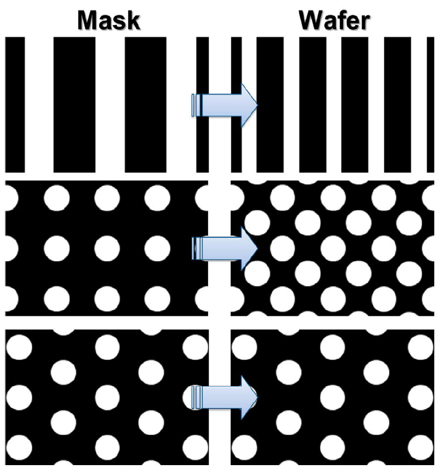
Both, one-dimensional patterns, such as lines and spaces, and two-dimensional patterns, such as hexagonal or square lattices can be produced. Examples of patterns printed using this method are shown in figure 2. The mask features are shown on the left, while the printed resist images are presented on the right. One advantage that can be seen is the demagnification ability for some cases. Taking a closer look at the lines and spaces on the top, the demagnification has a factor of 2. In the case of a square lattice, a feature in the center of the square lattice is printed simultaneously, giving printed image which has a demagnification of √2:1 and a rotation of 45°. In case of a hexagonal lattice, the periodicity of the patterns on the mask and the wafer are equal. This factor of demagnification is an inherent property of the diffraction nature of this process.
 and resulting print images on the wafer (right) for lines (top), square arrays (middle) and hexagonal arrays (bottom)") Figure 2: Schematics of the feature size correlation between mask structures (left) and resulting print images on the wafer (right) for lines (top), square arrays (middle) and hexagonal arrays (bottom)
Figure 2: Schematics of the feature size correlation between mask structures (left) and resulting print images on the wafer (right) for lines (top), square arrays (middle) and hexagonal arrays (bottom)
After taking a detailed look at the printing properties, the discussed printing capabilities are demonstrated. Figure 3 gives a selection of printed nano-patterns, marking the lower end of the printing resolution for lines and space, square and hexagonal arrays at the given parameters. Evaluation of the printed structures showed that good uniformity and reproducibility were obtained despite an uneven gap and large resist thickness, proving that the pattern is indeed insensitive to the distance between mask and wafer.
, square array with a hole diameter of 175 nm (b) and 250 nm pitch and (c) hexagonal array with a hole diameter of 260 nm (c)") Figure 3: SEM images of photonic patterns printed with PHABLE: lines and spaces with 125 nm half pitch (a), square array with a hole diameter of 175 nm (b) and 250 nm pitch and (c) hexagonal array with a hole diameter of 260 nm (c)
Figure 3: SEM images of photonic patterns printed with PHABLE: lines and spaces with 125 nm half pitch (a), square array with a hole diameter of 175 nm (b) and 250 nm pitch and (c) hexagonal array with a hole diameter of 260 nm (c)
Sub-resolution nano-scale patterns receive wide interest for all kinds of photonic applications. Nevertheless, larger micrometer-scale structures are also frequently demanded. For PSS the features are in the range of 2 μm. Just the same as nPSS, PSS structures have been replicated (Figure 4). as well as holes (b) of the same sizes can be replicated with the same mask, by changing the resist type from positive to negative exposure type") Figure 4: SEM images of resist pillars for patterned sapphire substrates. Pillar sizes of 2.0 μm (a) as well as holes (b) of the same sizes can be replicated with the same mask, by changing the resist type from positive to negative exposure type
Figure 4: SEM images of resist pillars for patterned sapphire substrates. Pillar sizes of 2.0 μm (a) as well as holes (b) of the same sizes can be replicated with the same mask, by changing the resist type from positive to negative exposure type
Process variability and control
Pattern size in photonics varies in a wide range and precise control is important. In contrast to other patterning technologies PHABLE offers a broad window of pattern size control. On the one hand, resist pattern height adjustment is straight forward. Due to the ideal two-dimensional exposure region it is independent of the lithography process and simply controlled by resist thickness. Standard i-line and broad band resists are well established in semiconductor fabs and their coating performance and thickness are optimized. On the other hand, PHABLE has a unique property to control lateral feature dimensions. Just by changing the exposure dose, feature sizes can be tailored within a wide range, as shown in figure 5. The exposure integration through sample movement, does not influence sidewall shape or angle of the via openings in resist and resist pillars. In short, the same mask for hexagonal pillar sizes of 250 nm can also produce 350 nm pillars. Further control of the printed pattern can be obtained by optimization of the mask pattern and illumination field distribution, to produce more delicate features than circles in the unit cell of the image. In addition, the large gap between the mask and the wafer avoids contact and damage and contamination and ensures an extremely long lifetime for the masks. This directly transfers into a clear cost advantage compared to other technologies.
 Figure 5: SEM images of substrate patterned by using the same mask but varying exposure dose. The relation between exposure dose and hole diameter is tunable over a wide range, resulting in a wide process control
Conclusion and Outlook
Printing of photonic structures is one of the key features for PHABLE. LED wafers have some extreme properties, such as high bow, warp and high surface defect density. Photonic nanostructures can be created on LED surfaces after epitaxial deposition steps or on sapphire substrates before the device layers are grown.
This new technology is ideally suited for patterning either structure. In particular, its non-contact nature and ability to print across large topographical features including uneven surfaces are highlights. Furthermore, a very wide range of feature sizes can be printed with the same tool. This does not only apply to different masks, but many different patterns can even be simultaneously printed on a single chip or wafer, making it a highly versatile and flexible tool for current and future production needs.
Full List of Authors:
* Thomas Uhrman, Alois Malzer, Alberto Montaigne Ramil, Boris Považay, Roman Holly, Thorsten Matthias, Markus Wimlinger, Paul Lindner, EV Group; Harun H. Solak, Christian Dais, Francis Clube, Peter Cairoli, Eulitha AG
References:
[1] J.J. Chen, et. al., “Enhanced Output Power of GaN-Based LEDs With Nano-Patterned Sapphire Substrates”, IEEE Electronics Technology Letters, Vol. 20, p.1195 (2008)
[2] Y.-K. Ee, et. al., “Metalorganic Vapor Phase Epitaxy of III-Nitride Light-Emitting Diodes on Nanopatterned AGOG Sapphire Substrate by Abbreviated Growth Mode”, IEEE Journal of Selected Topics in Quantum Electronics, Vol. 15 , p.1066 (2009)
[3] Y.-K. Ee, et. al., “Abbreviated MOVPE nucleation of III-nitride light-emitting diodes on nano-patterned sapphire”, Journal of Crystal Growth, Vol. 312, p.1311 (2010)
[4] M. Ma, et. al., “Strong light-extraction enhancement in GaInN light-emitting diodes patterned with TiO2 micro-pillars with tapered sidewalls”, Applied Physics Letters, Vol. 101, p.141105 (2012)
[5] H. Solak, C. Dais, F. Clube, ”Displacement Talbot lithography: a new method for high-resolution patterning of large areas”, Optics Express, Vol. 19, p.10686 (2011)
