Roll-to-Roll UV Nanoimprint Lithography for Large-Area Nano- and Micro-Structuring of Flexible Substrates
LpR 67 Article, page 50: Cost and time-efficient methods for the fabrication of optical elements are highly desirable in the field of lighting. Imprinting optical structures in combination with large area fabrication turns out to become an effective approach in this regard. In particular roll-to-roll UV nanoimprint lithography (R2R-UV-NIL) has a large potential to set new benchmarks for the fabrication of miniaturized, low-cost and low-weight optics that can be applied in many fields of applications. In the following, the Joanneum Research Forschungsgesellschaft m.b.H team, Claude Leiner, Stephan Ruttloff, Dieter Nees, Anja Haase, Ladislav Kuna, Wolfgang Nemitz, Franz-Peter Wenzl, Christian Sommer, Barbara Stadlober and Ursula Palfinger, led by Paul Hartmann, demonstrates the maturity of the related process chain, combining optical design, direct laser lithography, step&repeat imprinting for shim fabrication and R2R reproduction.
During the last few years, light emitting diodes (LEDs) have conquered almost all segments of the lighting market as a consequence of the manifold of advantages they provide, ranging from long lifetime, reliability, energy saving, light and color control to new possibilities for system integration. Their compact size also allows the use of tailored primary and secondary optical elements to generate arbitrary radiation patterns, in particular in case of freeform (FF) optical elements, or to couple and to guide the light in accordance with demands. These optical elements may have dimensions of centimeters down to millimeters and a variety of methods for their fabrication are applied owing to the complexity of the optical elements and the required precision. Examples in this regard range from injection molding to ultra precision diamond machining. However, a lot of these methods are comparably expensive and suchlike fabricated optical elements account for a notable percentage to the costs of a luminaire. Therefore, more cost and time-efficient methods for the fabrication of such optical elements are highly desirable. One such fabrication method could be imprinting of optical structures, ideally using roll-to-roll (R2R) processes for large-scale fabrication. However, imprinting is limited to fabrication of optical elements with much smaller sizes than the ones typically used for lighting. On the other hand such ultrathin, foil-based optical elements also offer, besides their low height, additional benefits, including ease of system integration and reduced weight.
The Fabrication Procedure
The process described below allows for the fabrication of tailored optical structures cost and time-efficiently by an approach that is based on master fabrication by mask-less gray scale laser lithography and the replication from these masters using step&repeat imprinting for shim fabrication. This shim can then be used as a stamp for R2R reproduction. Exemplarily, the fabrication of ultrathin freeform micro-optical elements on foils will be shown. Such foils can be directly integrated into the light sources or they can be laminated, e.g., on optically transparent plates.
The design procedure for the ultrathin FF micro-optical elements has been published in more detail elsewhere [1, 2]. It enables realization of (freeform micro-) optical elements with heights of several 10 μm that provide radiation patterns on a target plane as desired. In order to generate such ultrathin FF lenses a sophisticated algorithm for calculating the freeform surface was implemented, including the introduction of minimal and maximal thresholds of the freeform. Figure 1 shows a cross-section along one half of the diameter of such an FF micro-optical element that was designed to provide a rotationally symmetric radiation pattern. Also the 3D model of the FF micro-optical element is shown in the figure.
, and 3D model of the FF microoptical element (b)") Figures 1a&b: Cross-section along one half of the diameter of the FF micro-optical element (a), and 3D model of the FF microoptical element (b)
Figures 1a&b: Cross-section along one half of the diameter of the FF micro-optical element (a), and 3D model of the FF microoptical element (b)
Figure 2 shows the predicted light intensity distribution on a target plane using the FF micro-optical element of figure 1 in combination with an LED light source as well as an image showing a wall that is illuminated by an LED through the FF micro-optical element. The latter one was fabricated in a batch process [3]. The sag height of the FF micro-optical element is about 60 μm and the diameter of the element is about 10.75 mm.
 Figures 2a&b: Light intensity distribution on the target plane using the FF micro-optical element in combination with an LED light source, simulation (a), experiment with a wall representing the target plane (b)
Still, the procedure can also be extended to design non-rotationally symmetric irradiance distributions with, e.g., an irradiance distribution having a square shape. In this case the FF object has to be “segmented” into different slices with a constant azimuth step size, as shown in figure 3 and discussed in detail in [2].
 Figures 3a&b: Cross-sections along one half of the diameters of a FF microoptical element (a) and a (98 segments) 3D Model (b) designed for generating a uniform irradiance distribution with a square shape on a target plane
The R2R-UV-NIL Process
Besides their compactness and low weight, the main benefit of such structures is the possibility to fabricate them on a large scale in an R2R process. In this regard R2R-UV-NIL is one of the most promising high-resolution patterning techniques that can account for cost-effective large-scale production on flexible substrates [4]. Initially demonstrated for thermal imprinting in 1998 by Tan et al. [5], Ahn et al. [6] extended its potentials to R2R-UV-NIL. While for thermal imprinting a thermoplastic material is embossed at temperatures above its glass transition and hardened by subsequent cooling, in UV-NIL the desired structure is transferred by a stamp into an imprint resist and fixed simultaneously by UV-curing.
With R2R-NIL the flat and rigid stamps that are used for a lot of other imprinting processes are replaced by roller stamps. This has the advantages that the imprinting is done continuously, which allows for a more homogeneous and conformal pressure application, improved resist displacement, seamless pattern transfer and high throughput. Such roller stamps can be either patterned rolling cylinders with either a metallic or silicone surface, or bendable patterned stamps that are wrapped around a metal roller [4]. Such flexible stamps, named “shims” can be easily attached on and detached from the roller.
The whole process chain for R2R fabrication of micro-scaled optical structures therefore comprises the aforementioned optical simulations, the fabrication of a master in accordance with the optical design, up-scaling of the master for the fabrication of a polymer shim and finally roll-to-roll fabrication. From a viewpoint of optical design and the complexity of the optical structures, larger heights would be preferable. On the other hand, from the viewpoints of laser lithography and R2R-NIL fabrication, smaller heights are preferable. Therefore, in dependence of the complexity of the structures a certain compromise with respect to the final height have to be made for which the aforementioned implementation of an additional algorithm in the design process that allows to define arbitrarily threshold values for the final height of a specific structure, is an essential step to align simulation and fabrication.
The process chain for the fabrication of the simulated structures is shown in figure 4.
 Figure 4: Process chain for the R2R-UV-NIL based fabrication of optical structures. The main steps are master fabrication (1), step&repeat (2-5) and R2R-UV-NIL (6-7)
Process chain for the R2RUV-NIL based fabrication
An effective method for the fabrication of masters for suchlike structures ((1) in Figure 4) is a mask-less laser direct write lithography (MALA) approach, which is based on gray-scale direct laser lithography [3].
Besides the laser writing process itself, the most relevant part of master fabrication is the generation of a “virtual” photomask. The virtual photomask, which is directly generated from the 3D model of the FF micro-optical element, specifies the respective light dosage that is applied at a given XY-position of a stage on which the sample is placed. This light dosage can be varied while scanning the laser beam across the sample in accordance with the desired structure to be fabricated.
The whole process is schematically illustrated in figure 5, the operating mode of the MALA process in figure 6.
") Figure 5: Schematic of the fabrication of the master by mask-less laser direct write lithography (MALA)
Figure 5: Schematic of the fabrication of the master by mask-less laser direct write lithography (MALA)
 Figure 6: Scheme of the operating mode of the MALA process
The next step ((2-5) in Figure 4) is the up-scaling of the master to a shim by step&repeat equipment. This tool allows very fast up-scaling of the written structures to larger sized masters and shims for R2R processes by highly precise stitching of the pattern elements of the master structure. For this, the master template is replicated by imprinting its pattern to a working stamp, which is used for the actual step and repeat processing ((2) in Figure 4). Using such an approach, the lifetime of the master template can be largely prolonged. In the step&repeat process a UV curable resist is applied to the substrate (3). The transparent working stamp then comes into contact with the substrate. In a subsequent step the resist is cured with UV light (4). Finally, the working stamp is released (5) and reused for the next print, close to the previously set structure.
Figure 7 shows an image of the step&repeat equipment. Figure 8 is an image of a shim that was fabricated from the master template of free-form micro-optical elements, after metallization. Once the shim is fabricated the shim can be used for large-scale replication by R2R-UVNIL (6-7 in Figure 4).
 Figure 7: Image of the step&repeat equipment
 Figure 8: Image of the shim fabricated by step&repeat with the free-form microoptical elements
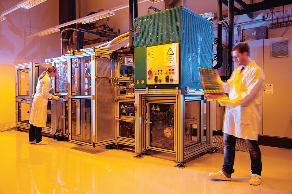
Proof of Concept in the Pilot Plant
Figure 9 shows an image of the R2R-UV-NIL pilot plant. For R2R fabrication a liquid UV-curable imprint resist is coated on a floating foil on a 250 mm wide web. The requirements on the specific imprinting resist used are many-fold ranging from good substrate adhesion over a high curing rate and low surface energy to sufficientlylow viscosity for fast spreading and filling of stamp cavities [4]. Still, a clear benefit is also that the resin composition can be varied and/or additives can be added to the resin, which allows for the modification of the refractive index of the structured layer. This allows much higher flexibility in exploiting all potential optical effects compared to thermal imprinting into a single polymer foil material.
 Figure 9: R2R-UV-NIL pilot plant at Joanneum Research in Weiz, Austria
On its way through the R2R machine, the coated foil passes the imprinting unit which contains the shim that is mounted on a steel roller. The pressure that is needed to transfer the topographic shim pattern into the resist is applied by a soft rubber-coated counter roller pressing the substrate against the shim ((7) in Figure 4).
Still, the alignment of structure design, resist parameters and process parameters is quite a complex process with a lot of mutual interferences that have to be aligned precisely to one another in order to allow for structures with high quality and precision. Improvements in this regard are ongoing; in particular with respect to the process speed for fabricating high quality R2R-UV-NIL imprinted free-form micro-optical elements. Figure 9 shows the current status, which allows the R2R fabrication of defect free structures with a process speed in the low m/min range, while structures fabricated at around 10 m/min still suffer from imperfections and embedded air bubbles.
Figures 10 show the free-form micro-optical elements fabricated by R2R-UV-NIL at different speeds, and finally, figures 11 shows a final roll with free-form micro-optical elements as well as a further example with light-coupling structures.
") Figures 10: Free-form micro-optical elements fabricated by R2R-UV-NIL at different speeds(left: 10 m/min| right: 1 m/min)
Figures 10: Free-form micro-optical elements fabricated by R2R-UV-NIL at different speeds(left: 10 m/min| right: 1 m/min)
 light coupling structures and (right) free-form micro optical elements fabricated by R2R-UV-NIL") Figures 11: Final rolls with (left) light coupling structures and (right) free-form micro optical elements fabricated by R2R-UV-NIL
Figures 11: Final rolls with (left) light coupling structures and (right) free-form micro optical elements fabricated by R2R-UV-NIL
Conclusions
Still a young technology, all these examples demonstrate that owing to the progress over the last years R2R-UV-NIL and the related process chain has become a mature technology for cost- and timeeffective large scale fabrication of optical elements. Such miniaturized, low-cost and low-weight optics will have a huge impact in the coming years not only for lighting, but also for a lot of other applications in that optical structures are core elements.
References:
[1] C. Leiner, W. Nemitz, S. Schweitzer, F. P. Wenzl, C. Sommer,
„Smart freeform optics solution for an extremely thin direct-lit
application”, Proc. of SPIE 9889, 988911 (2016)
[2] C. Leiner, W. Nemitz, S. Schweitzer, F. P. Wenzl, L. Kuna, F. Reil,
P. Hartmann, C. Sommer, „Thin direct-lit application for general lighting
realized by freeform micro-optical elements”, Proc. of SPIE SPIE 9955
99550E (2016)
[3] L. Kuna; C. Leiner; W. Nemitz; F. Reil; P. Hartmann; F.P. Wenzl;
C. Sommer, Optical design of freeform micro-optical elements and their
fabrication combining maskless laser direct write lithography and
replication by imprinting, J. Photon. Energy. 7, 016002, (2017)
[4] M. Leitgeb, D. Nees, S. Ruttloff, U. Palfinger, J. Götz, R. Liska,
M. R. Belegratis, B. Stadlober, Multilength Scale Patterning of
Functional Layers by Roll-to-Roll Ultraviolet-Light-Assisted Nanoimprint
Lithography, ACS Nano 10, 4926−4941, (2016)
[5] H. Tan, A. Gilbertson, S. Y. Chou, Roller Nanoimprint Lithography,
J. Vac. Sci. Technol., B: Microelectron. Process. Phenom. 16,
3926 - 3928, (1998)
[6] S. Ahn, J. Cha, H. Myung, S.-M. Kim, S. Kang, Continuous Ultraviolet
Roll Nanoimprinting Process for Replicating Large-Scale Nano-
and Micropatterns. Appl. Phys. Lett. 89, 213101. (2006)
