Semi-Empirical Characterization of Freeform Microlens Arrays
LpR 72 Article - page 42: Microlens arrays (MLA) have been used for imaging and non-imaging applications for a long time as cost-effective solutions. Non-symmetrical beam shapes require more advanced non-symmetrical freeform microlens arrays (FMLA). The required FMLA molding tools convey a high cost and an iteration process is required for the final design. Oscar Fernández, Tamara Aderneuer, Rolando Ferrini from the Centre Suisse d'Electronique et de Microtechnique, CSEM, and Julien Duchene from ANSYS proposed a method to overcome these limitations based on 3D surface sampling, computer generation of a ray-traceable model and ray-tracing performance simulation and demonstrate feasibility for several commercially available freeform asymmetric thin-film diffusers.
The practical advantages of microlens arrays, MLAs, have been widely exploited in diverse applications such as illumination, imaging, optical communication and security/anti-counterfeiting. On the other hand, the advances in computing and ultra-precision micro-machining achieved in the last years have enabled the design and manufacturing of the so-called freeform optical components. Such components, with no restrictions in rotational or translational symmetry, represent a fundamental shift and a powerful tool for optical designers and engineers to boost device miniaturization and performance, create new functionalities and reduce manufacturing costs.
Not surprisingly, freeform microlens arrays, FMLAs, are starting to attract attention both for imaging and non-imaging applications. However, the benefits enabled by the additional design freedom are accompanied by new challenges; being the lack of characterization methods a central one which, if not solved, will hinder progress and innovation in this tremendously promising technology.
In an attempt to bridge this gap, a characterization method based on the experimentally measured surface micro-relief and subsequent creation of a ray-traceable CAD model has been developed. The optical performance of the created solid is accurately predicted using ANSYS SPEOS®, an optical modelling software package developed by ANSYS, Inc. The built-in features of ANSYS SPEOS enabled simulations under different conditions without confronting the physical limitations encountered in real characterization setups.
The results presented here exemplify the advantages of the proposed method and highlight the need for further research in this topic.
Introduction
Microlens arrays, MLAs, defined as collections of microscopic lenses regularly arranged in a 1 or 2-dimensional pattern on a supporting substrate [1], offer several advantages when compared to macroscopic, single optical components, including miniaturization and manufacturing/ packaging cost reduction [2]. Additionally, the use of MLAs enabled opto-electronic devices with functionalities unreachable otherwise [3] such as integral photography, erect one-to-one imaging systems for photocopying and lithographic systems [4, 5], array generation for e.g. Shack-Hartmann wavefront sensors [6], etc.
Their microscopic surface relief enable microlens arrays, MLAs, to cover large areas with moderate volumes/weights, have a lower environmental footprint and retain substrate's flexibility, hence allowing replication over large areas using roll-based, cost-effective processes. Consequently, MLAs are commercially exploited today for, e.g. display brightness enhancement [7, 8], light extraction in LED [9] and OLED [10] lighting panels, beam homogenizers in LCD projectors [11], glare-free LED panels [12, 13] (Figure 1), intelligent windows [14, 15] and world-record concentration photovoltaics [16].
Moreover, MLAs are widely used to couple light into arrays of other optical components such as VCELs [17], CCD [18, 19] and LCD [20 - p.234] pixels and optical fibers for optical interconnections [4, 21]. Other advantages of MLAs include low heat production and mechanical inertia, high resistance to vibrations [22]. Finally, their invisibility to the naked eye make them very appropriate for security [23-25] and packaging [26] applications.
Remarkably, many applications require non-symmetrical light outputs. For example, commonly used image sensors are rectangular. Also, uniform illumination over rectangular targets (e.g. office tables, roads, and supermarket racks) is also a common goal in artificial lighting. In these cases, freeform optical surfaces, designed with no symmetry constraints, offer more efficient light utilization [27-29].
Furthermore, appropriately designed freeform components have higher ability to control Seidel aberrations independently, thus increasing the resolution, field of view and f-number coverage of imaging devices [30]. Finally, single freeform FMLAs can replace several MLAs hence reducing manufacturing and integration costs [31-36].
Freeform microlens arrays, FMLAs, which combine the design freedom of freeforms with the microscopic nature of micro-optics, are currently exploited in commercial applications such as laser beam-shapers and homogenizers [37] and asymmetric light diffusers [12]. On the other hand, FMLAs have enabled the design of compact monolithic imaging systems with high resolution and signal-to-noise, minimum off-axis aberrations, high signal-to-noise and large field of view [38-41]. 3D light-field displays and cameras [42-45] and see-through head-mounted glasses [46].
The Proposed Method
As a flip side, the use of freeforms optics conveys specific challenges in terms of design, manufacturing and characterization [2]. The latter aspect, which has received much less attention, is fundamental for the success of FMLA technology and is the focus of this work.
A common approach to characterize MLAs is to measure the surface profile using, e.g., an optical profilometer and compare the results with the prescribed design target. MLAs are usually characterized by few parameters - residual layer, sag, pitch and fill factor and the impact of observed form error on the optical performance can be easily estimated. However, freeform surfaces are described by a much larger parameter space and oftentimes by non-parametric sets of points [37]. As a result, quantifying the form error and the resulting performance degradation is noticeably more complex.
FMLA tools are costly to manufacture and very small samples are typically produced (and subsequently steeped-and-repeated to produce the final large-area masters). Small samples are, however, difficult to handle and their characterization is prone to large experimental errors due to equipment and alignment limitations.
Both issues can be circumvented using a semi-empirical approach, which comprised two main steps. Firstly, the surface profile was recorded over a surface large enough to contain a significant number of microstructures (typically few mm2) and used to build ray-traceable CAD solid. Unfortunately, the whole process necessitated several intermediate format conversions (Figure 2) using different CAD software packages. The data provided by the profilometer had first to be transformed to a standard (.xyz) point-cloud format using an in-house model-based development software and thereafter converted into a Non-Uniform Rational B-spline (NURBS) surface, exported as .IGS format using RESURF point-cloud-to-NURBS fitting software [i] and finally imported into SolidWorks [ii] where it was extruded to the desired thickness and knitted to render solid properties to the model [iii].
In a second step, the optical performance of the built model was imported into a ray-tracing simulation tool and its performance simulated under preset conditions. ANSYS SPEOS [iv] is fully embedded into SolidWorks and is an excellent tool for our purpose. In addition, it offers a plethora of built-in features (in addition to those built-in within the SolidWorks environment) including, for example, an extensive library of experimentally characterized light sources and materials, a wide range of detectors, and several data analysis packages (Figure 3).

Figure 2: Schematic view of the process chain used in the creation of a a ray-traceable CAD model from the measured surface profile
Results
We applied the described method to characterize the following FMLA-based thin-film solutions:
• Polyscale light defining film[v]
• RPC Photonics ED-S50 engineered diffuser [vi]
• BrightView E1060 asymmetric diffuser [vii]
• BrightView glare control diffuser G-GC90 [viii]
In the first 3 cases the CAD models were exposed to a highly collimated illumination and the irradiance recorded by a planar detector located at 100 mm from the sample (Figure 3). As a reality check the real samples were illuminated using a green laser and the illuminated target photographed. The results shown in figures 4 & 5 (left) clearly show the great agreement between the CAD models and SEM pictures as well as between the predicted and observed optical performance.
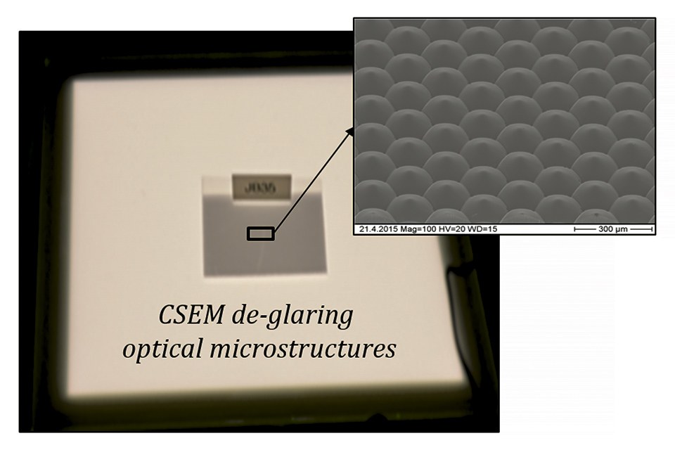
The CAD-model of the BrightView G-GC90 foil was illuminated by a flat Lambertian white light source and the luminous intensity measured using ANSYS SPEOS far-field polar EULUMDAT detector (Figure 3). The real sample was measured in combination with an OLED lighting device (PhillipsLF300) and the intensity distribution curve measured using a gonio-photospectrometer well beyond the far-field conditions in the C0-C180 plane. Again, the comparison, shown in figure 5 - right, shows a great agreement.
Conclusions
FMLA technology is a powerful tool for optical design in many different applications fields. Since it is still at an early stage, this technology can progress much beyond its current status. However, further development can easily be frustrated by the lack of appropriate metrology solutions.
With support from advanced simulation tools such as ANSYS SPEOS semi-empirical procedures are possible for which, according to the results presented here, there is a large potential for the efficient and accurate characterization of FMLAs. Three aspects must nonetheless be addressed before we can fully evaluate the merit of the proposed method.

Figure 3: Optical set-up created in ANSYS SPEOS for the simulation of a CAD model illuminated by a collimated, monochromatic green light source. The resulting intensity and irradiance distributions produced by the solid are measured by the polar EULUMDAT and planar IRRADIANCE detectors respectively
 and simulated and experimental irradiance distributions under laser illumination (bottom).")
Figures 4a&b: CAD models and SEM pictures (top) and simulated and experimental irradiance distributions under laser illumination (bottom). Polyscale defining film (a). RCP Photonics ED-S50 (b)

Figure 5: CAD models and SEM picture and predicted versus observed performance (left) of a BrightView E1060 asymmetric diffuser. BrightView G-CG90 de-glaring foil (right). Predicted and measured luminous intensity of a de-glared Phillips LF300 OLED (bottom-right)
The lack of standard formats to describe FMLAs imposes multiple intermediate format conversions steps using different software tools, which not only is rather inconvenient but also susceptible to cumulative errors. The authors believe that efforts towards the standardization of the FMLAs will not only facilitate their characterization but also allow a better interface and improve the communication and mutual understanding between optical designers and manufacturers.
On the other hand, although we have so far restricted the study to qualitative comparisons, a full evaluation of the method demands for quantitative tests. Such work is planned at CSEM and the results will be reported elsewhere.
Finally, it must be mentioned that this work has focused solely on form accuracy and ignored effects arising from the non-negligible roughness of the involved surfaces and their optical effects, primarily specular reflectivity and light scattering [47]. On one size, the profilometer used for this work cannot measure sub-micron features with good lateral resolution. This could be addressed using more precise surface profilers (e.g. AFM, SEM, white-light interferometers and confocal laser microscopes) albeit the increase in the point density and the concomitant complexity of the resulting CAD model would need to be handled appropriately.
Notes:
[I] http://www.resurf3d.com/Pointcloud2Nurbs.htm
[ii] https://www.solidworks.com/
[iii] Attempts to convert the point-cloud directly in SolidWorks using the
ScanTo3D add-in rendered meshes with a large number of errors
including holes, faulty surface normals and self-intersections.
[iv] https://www.ansys.com/products/optical/ansys-speos
[v] https://polyscale.com/en/products/optical-films/
[vi] https://www.rpcphotonics.com/product/eds-50/
[vii] https: // www.brightviewtechnologies.com/products/led-diffusers/elliptical-led-diffusers/page.aspx?id=1121
[viii] https://www.brightviewtechnologies.com/products/light-management/glare-control-diffusers/page.aspx?id=1132
References:
[1] Zappe, H. (2012). Micro-optics: a micro-tutorial. Advanced Optical
Technologies, Vol. 1, No. 3; pp. 117-126;
[2] Reinhard Völkel (2012). Wafer-scale micro-optics fabrication.
Advanced Optical Technologies, Vol. 1, No. 3; pp. 135-150
[3] T. Zhou, X. Liu, Z. Liang, y. Liu, J. Xie and X. Wang (2017). Recent
advancements in optical microstructure fabrication through glass
molding process, Front. Mech. Eng. Vol. 12, No. 1; pp. 46-65
[4] Hutley, M, Stevens R. and Daly, D (1991). Microlens arrays,
Physics World, 4 (7), pp. 27-32
[5] Reinhard Völkel, Hans Peter Herzig, Philippe Nussbaum,
Rene Dandliker and William B. Hugle (1996). Microlens array imaging
system for photolithography, Opt. Eng. 35 (11), pp. 3323 – 3330
[6] Tingxiu Hou, Chong Zheng, Shi Bai, Qian Ma, Denzel Bridges,
Anming Hu, and W. W. Duley. Fabrication, characterization,
and applications of microlenses, Appl. Opt. 54, 7366-7376 (2015)
[7] https://www.3m.com/3M/en_US/industrial-manufacturing-us/display-enhancement-and-protection-films-industrial-manufacturing/display-enhancement-films/
[8] Ruidong Zhu, Qi Hong, Yating Gao, Zhenyue Luo, Shin-Tson Wu,
Ming-Chun Li, Seok-Lyul Lee, and Wen-Ching Tsai (2015). Tailoring the
light distribution of liquid crystal display with freeform engineered
diffuser, Opt. Express Vol. 23, No. 11; pp. 14070-14084
[9] James Gourlay (2015). Making Light Work – Light Sources for Modern
Lighting Requirements, LED Professional Review, Issue 47; pp. 72-75
[10] Hyun Soo Kim, Seong Il Moon, Dong Eui Hwang, Ki Won Jeong, Chang Kyo Kim, Dae-Gyu Moon Chinsoo Hong (2016). Novel fabrication method of microlens arrays with High OLED outcoupling efficiency, Optics & Laser Technology, Vol. 77; pp. 104-110
[11] Jui-Wen Pan, Chih-Ming Wang, Hsiao-Chin Lan, Wen-Shin Sun,
and Jenq-Yang Chang (2007). Homogenized LED-illumination using
microlens arrays for a pocket-sized projector, Opt. Express Vol. 15,
No. 17; p. 10483
[12] https://www.brightviewtechnologies.com/
[13] K. Reutter, O. Fernandez, R. Ferrini, C. Hochfilzer and T. Dreyfus,
OPTICAL FILM AND LIGHT FIXTURE WITH SUCH AN OPTICAL
FILM; WO2017050929 (A1) ― 2017-03-30
[14] Selin Ashaboglu, Object of the Moment: 3M Daylight Redirecting Film
by 3M, Architectural lighting, daylighting and solar control, March 02
(2017). Available on-line: https://www.archlighting.com/products/daylighting-and-solar-control/object-of-the-moment-3m-daylight-redirecting-film-by-3m_s
[15] Helmut F.O. Mueller (2017). Micro-optical structures for daylighting and
led systems, Renew. Energy Environ. Sustain. Vol. 2, No. 29;
DOI: 10.1051/rees/2017044
[16] New World Record for Concentrator Photovoltaics – 36.7 Percent for
New Solar Module Using Highly Efficient Multi-Junction Solar Cells.
https://www.ise.fraunhofer.de/en/press-media/press-releases/2014/new-world-record-for-concentrator-photovoltaics.html
[17] V. Bardinal, T. Camps, B. Reig, D. Barat, E. Daran and J. B. Doucet
(2011). Collective Micro-Optics Technologies for VCSEL Photonic
Integration, Advances in Optical Technologies, Article ID 609643,
11 pages; doi:10.1155/2011/609643
[18] http://hamamatsu.magnet.fsu.edu/articles/microlensarray.html
[19] Leica announces M10 with new sensor, slimmer design, DPReview.
Available online: https://www.dpreview.com/news/8915550991/leica-announces-m10-with-new-sensor-slimmer-design
[20] N. F. Borelli (2005), Microoptics Technology, Marcel Dekker
[21] Reinhard Voelkl, Andreas Bich and Kenneth J. Weible and Maik
Zimmermann (2008). Highly efficient array generators based on
modern micro optics. Dimensionally accurate micro optics,
Optolines No. 16; pp.12-14
[22] Boswell, B., Islam, M.N. & Davies I.J (2018). A review of micro-
mechanical cutting, Int. J. Adv. Manuf. Technol. 94: 789
[23] Svyatoslav Voloshynovskiy, Maurits Diephuis, Taras Holotyak,
and Nabil Standardo (2014). Physical object identification using micro-
structure images, SPIE Newsroom. DOI: 10.1117/2.1201411.005524
[24] S. Palm (2012). Micro-optics technology for ID applications.
Promising overt banknote security feature for use in secure
documents, Keesing Journal of Documents & Identity, June 2012, pp. 1-3.
[25] Richard A. Steenblik, Mark J. Hurt, Michael E. Knotts (2002).
Advantages of micro-optics over holograms for document
authentication, Proceedings Volume 4677, Optical Security and
Counterfeit Deterrence Techniques IV
[26] http://www.fresnelsinc.com/products.html
[27] P. Benitez and J. C. Miñano. The Future of Illumination Design,
OPN May 2007 pp.20-25
[28] Fabian Duerr, Youri Meuret, and Hugo Thienpont. Potential benefits of
free-form optics in on-axis imaging applications with high aspect ratio,
Opt. Express 21, 31072-31081 (2013)
[29] E. Chen, R. Wu and T. Guo (2014). Design a freeform microlens array
module for any arbitrary-shape collimated beam shaping and color
mixing, Optics Communications 321; pp. 78–85
[30] Kevin P. Thompson and Jannick P. Rolland (2012). Freeform Optical
Surfaces: A Revolution in Imaging Optical Design, Optics & Photonics
News Vol. 23, No. 6; pp. 30-35
[31] L. Li and A. Y. Yi (2011). Design and fabrication of a freeform microlens
array for uniform beam shaping, Microsyst. Technol., 17:1713–1720;
DOI 10.1007/s00542-011-1359-y
[32] F.Z. Fang, X.D. Zhang, A. Weckenmann, G.X. Zhang, C. Evans
(2013). Manufacturing and measurement of freeform optics, CIRP
Annals - Manufacturing Technology, Vol. 62, pp. 823–846
[33] Fang, F., Zhang, N. & Zhang, X. (2016). Precision injection molding of
freeform optics. Advanced Optical Technologies, Vol. 5, No. 4,
pp. 303-324; doi:10.1515/aot-2016-0033
[34] Jingfei Ye, Lu Chen, Xinhua Li, Qun Yuan, Zhishan Gao (2017).
Review of optical freeform surface representation technique and its
application, Optical Engineering, Vol. 56, No. 11; p. 110901
[35] Timmo Gissibl, Simon Thiele, Alois Herkommer and Harald Giessen
(2016). Sub-micrometer accurate free-form optics by three-
dimensional printing on single-mode fibres, Nature Communications 7,
article number: 11763
[36] A. Broemel, U. Lippmann and H. Gross (2017). Freeform surface
descriptions – part I: Mathematical representations, Adv. Opt. Techn.
Vol. 6, No. 5; pp. 327-336
[37] Tasso RM Sales, Stephen Chakmakjian, G. Michael Morris and Donald
J. Schertler (2004), Light Tamers. Engineered microlens arrays provide
new control for display and lighting applications, Photonics Spectra,
June Issue. Available on-line:
https://www.rpcphotonics.com/pdfs/Light_Tamers.pdf
[38] Lei Li and Allen Y. Yi (2012). Design and fabrication of a freeform
microlens array for a compact large-field-of-view compound-eye
camera, Appl. Opt. Vol. 51; pp. 1843-1852
[39] Hao Zhang, Lei Li, David L. McCray, Sebastian Scheiding,
Neil J. Naples, Andreas Gebhardt, Stefan Risse, Ramona Eberhardt,
Andreas Tunnermann and Allen Y. Yi (2013). Development of a low
cost high precision three-layer 3D artificial compound eye,
Opt. Express, Vol. 21, No. 19; DOI:10.1364/OE.21.022232
[40] J. Dunkel, F. Wippermann, A. Reimann, A. Brückner and A. Bräuer
(2015). Fabrication of microoptical freeform arrays on wafer level for
imaging applications, Opt. Express, | Vol. 23, No. 25 |
DOI:10.1364/OE.23.031915
[41] Simon Thiele, Kathrin Arzenbacher, Timo Gissibl, Harald Giessen,
Alois M. Herkommer (2017). 3D-printed eagle eye: Compound
microlens system for foveated imaging, Sci. Adv.2017; 3 e1602655 15
[42] Nikhil Balram and Ivana Tošić (2016). Light-Field Imaging and Display
Systems, Information Display Vol. 32, No. 4; pp. 6-13
[43] http://www.fovi3d.com/
[44] Bader Aldalali, Chenhui Li, Li Zhang and Hongrui Jiang (2012).
Micro Cameras Capable of Multiple Viewpoint Imaging Utilizing
Photoresist Microlens Arrays, J. Microelectromechanical Systems,
Vol. 21, No. 4; pp. 945-952
[45] W. Yuan, L‑H. Li, W‑B. Lee and C‑Y Chan (2018). Fabrication of
Microlens Array and Its Application: A Review, J. Mech. Eng. 31:16;
https://doi.org/10.1186/s10033-018-0204-y
[46] H. Hua and B. Javidi (2015). Augmented Reality: Easy on the eyes
(2015), Optics & Photonics News, Vol. 26, No.2; pp. 26-33
[47] S. Singh, H. Solak, and F. Cerrina (1996). Multilayer roughness and
image formation in the Schwarzschild objective, Review of Scientific
Instruments Vol. 67, No. 9; pp. 3355 - 3355;
https://doi.org/10.1063/1.1147374
