Smart LED System in Package through Wafer Level Integration Approach
It is believed that LEDs will dominate all lighting applications in the near future. Integration and packaging are the two critical issues that, if resolved, will enable efficient and reliable solutions for lighting requirements. Z. Kolahdouz, H. van Zeijl, and G. Q. Zhang from the Institute of Microsystems and Nanoelectronics (DIMES) at the Delft University of Technology, and M. Kolahdouz from the Thin Film Laboratory and Nano-Electronics at the Department of Electrical and Computer Engineering of the University of Tehran show that wafer level packaging is a promising method to ensure lower cost, higher scale, and superior yield. A new integration approach of a smart unit of LED lighting is introduced: LED System in Package (SiP).
Emerging high power light emitting diodes (LEDs) was a key step for the development of new application areas in lighting [1-4]. The most common manufacturing approach for high power white LED source is the dichromatic method, which is also entitled as the phosphor-based white method. It is a combination of a short wavelength LED, such as blue or UV, and a phosphoric wavelength shifter. In the phosphor coating, a portion of photons are converted to yellow and the rest travel without any change. The light output is seen as a white light by human eyes [1-3]. This method shows good color rendering, long lifetime, and acceptable reliability over time. However, aging and high junction temperature affect the emitting wavelength and intensity [4-6]. This degradation may refer both to phosphor coating and LED chip performance over time. While the phosphor working mechanism is related to the manufacturing process [1], we can compensate LED aging and adjust its light intensity by controlling its driving current in a closed-loop system [7].
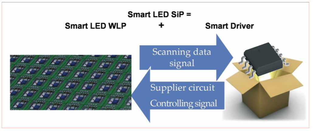 Figure 1: A smart LED system comprising a smart LED WLP and a smart driver
Silicon based Wafer Level Packaging (WLP) is the technology of choice for broad range of applications. This technology is a key in terms of cost and thermal design. It can provide batch fabrication and component integration, as it is compatible
with CMOS technology and thus, can include microelectromechanical system (MEMS) components as well [5, 6]. Applying these technologies, a smart LED package can be produced that resolves the brightness problems associated with LED intensity decay [6]. There are two categories of silicon-wafer-based WLP LEDs; the surface-mount type, in which electrodes are formed on a silicon wafer and then the LED chip is attached to the wafer; and the cavity type, in which cavities are formed prior to the electrodes [6]. Generally, the cavity is fabricated using KOH wet etching on a (100) silicon wafer. The cavity acts both as a reflector and a holder for filling phosphor and resin.
Another concern is large heat dissipation in such a high power package. Silicon wafer-level-package (WLP) can be a good solution for thermal management and a cost effective integration [6, 9, 10]. Using silicon-based infrastructures, IC technologies, and MEMS toolset and processes allow us to integrate different functional sub-blocks on the same die.
Monolithic integration of photonics and electronics in Si and other group IV elements was previously demonstrated [11-13]. Different groups reported integration of sensors and controlling blocks in Si-based LED WLP [6, 14-16]. However, developing a complete real-time light output controlling block in a low-cost process is still a point of interest.
In this article, a new integration approach of a smart unit of LED lighting is introduced: LED SiP. It comprises a smart LED wafer level package and a smart driver. This concept is depicted in Figure 1. Smart LED WLP is used as a Si based interposer for LED chips. Firstly, it integrates the wafer level optics, related interconnections, monitoring devices and powering circuits. An LED chip would be mounted later. In addition, to make the package smart and leverage semiconductor process, as much controlling functions as possible would be integrated into the silicon interposer. Smart driver is the brain of the total system. It works both as a driver circuit to supply power and a controller. By getting real time sensing data of the package, it can have better control over electrical and thermal management. Also, wireless communication and remote control functions can be included. Due to the rather large nature of LED chips, the final Si utilization yield of the interposer cannot get that high, but simple low cost processing can compensate the total cost of the package.
Smart LED SiP
The main focus of this article is on the smart WLP part. The final smart WLP is a high lumen output lighting module. It includes high current blue LEDs and different sensors in a reflector cavity. In this Si interposer with a high topography, lithography defined wiring is used as a reliable interconnect solution. Additionally, the control circuit of the LED output light was integrated on the same die to reduce costs of any required external circuitry. In more detail, the interposer monolithically integrates on-chip reflector cavity, sensors, remote phosphor layer, litho-defined wiring, power switching transistors, digital sensor readout circuit, and analog light feedback circuit into one smart LED WLP [17].
Different functions and operation levels of this system are presented in Figure 2.
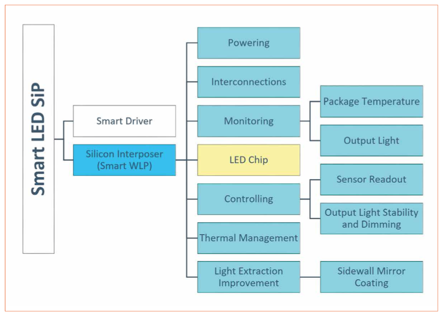 Figure 2: Different functions in a smart LED SiP (scope of this article is shown in color)
The advantages of such a LED SiP are:
• Capability of wafer-level optics
• Capability of wafer-level phosphor remote coating for stable color uniformity
• Higher brightness efficiency: on-chip reflector cup (cavity with mirror coating) reflects the sidelight and improves light extraction efficiency up to 15%
• Better thermal management: high thermal conductivity of Si substrate
• Lifetime improvement: self-monitoring system
• High reliability: better interconnect reliability, closed-loop feedback circuit for stability and aging compensation
To do so, BiCMOS 5-7 process was employed. It is a straightforward process that by just using 5-7 masks (corresponding to 1-2 metal layers) can monolithically implement different devices such as MOSFETs, BJTs, diodes, and resistors. The seven masks include N-well, N+ area, P+ area, contact opening, first metal, via opening, and second metal. Table 1 lists core of the process consists of 5-7 mask steps. A brief process overview is given in Figure 3. More details on BiCMOS process can be found in [7]. Due to large die size of LED chips, BiCMOS5/7 has a large potential to be utilized for WLP of smart LED systems [7, 18].
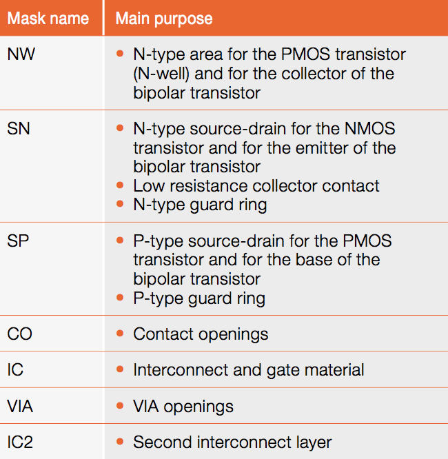 Table 1: Core process mask steps of the BICMOS5/7 process (the grey shaded ones are added for BiCOMS7)
Silicon-based WLP through low cost 7-mask BiCMOS process gives us the opportunity for integration of different passive and active components for a complete smart system. For sensing functions, thermal and optical sensors were implemented, characterized, and calibrated. Light measurement of the LED chip through the blue selective photodiode showed notable consistency to the LED datasheet values. Temperature sensors integrated just beneath LED chips, measuring the temperature in real time and the results were confirmed with IR photos. For controlling functions, a 4-bit flash ADC for reading out sensing output light, and a power switch for driving the LED current (up to 700 mA) were monolithically integrated. The reported components provides an essential platform for future work to have an analog or digital control system for any specific application. Furthermore, other technologies with large area demand such as Lab-on-Chip can benefit from this approach by utilizing smart silicon interposers. Figure 4 depicts some figures of 2D implementation of LED SiP.
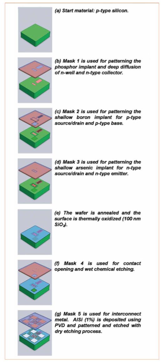 Figures 3 a-g: Process overview of the core steps in the BICMOS5 process
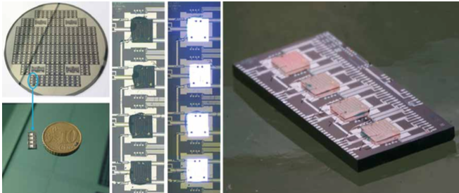 Figure 4: Monolithically integrated 2D LED SiP
A silicon stripe-shaped photodiode was designed and fabricated for sensing blue light in the LED wafer level package. The maximum responsivity was at 480 nm, which is matched with the blue LED’s illumination. This IC technology compatible photodiode, with junction at 330 nm, demonstrated a very high selectivity to blue light. The fabricated device presented a two-fold increase in the responsivity and quantum efficiency for blue light spectra compared to similar devices published earlier [7, 19]. The 3D schematic and the measured responsivity vs. wavelength are given in Figure 5(a) and (b), respectively.
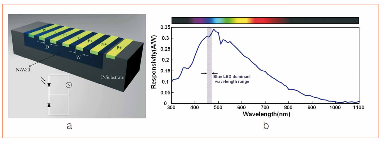 Figure 5a,b: 3D schematic of a blue selective photodiode (a), and responsivity vs. wavelength (b), measurement result (the patterned inset shows the dominant wavelength of the target LED)
To guarantee a stable light output that is linearly controllable with a reference input voltage, a monolithic light output feedback control circuit was integrated. It is also an appropriate solution for packaging a phosphor- based white LED module. Si-based wafer level smart control unit was integrated through our low-cost 7-mask BiCMOS process. For sensing blue/UV light in the package, the photodiode with its peak responsivity at 480nm wavelength was used. For controlling functions, a feedback circuit with a power transistor for driving the LED current was monolithically integrated. The opamp functionality was successfully tested with having 47 dB gain. The whole feedback circuit could regulate light output based on a reference voltage with removing power supply ripples even at very high frequencies (up to 680 kHz). Robustness of the feedback system was tested against changes in LED current/voltage to light intensity characteristics, which can be caused by aging or temperature changes. Considering a tight error tolerance of 1% for the light intensity, the system was able to handle up to 150 mA and 0.6 V change in current and voltage characteristic of the LED. Furthermore, it demonstrates the functionality of silicon based smart LED packaging with stable and regulated light output. This can also be applied to other smart systems like interposer for high-level electronics, MEMS, etc. Figure 6(a) illustrates complete schematic of the package with components used on its test board. The layout and chip micrograph is given in Figure 6(b).
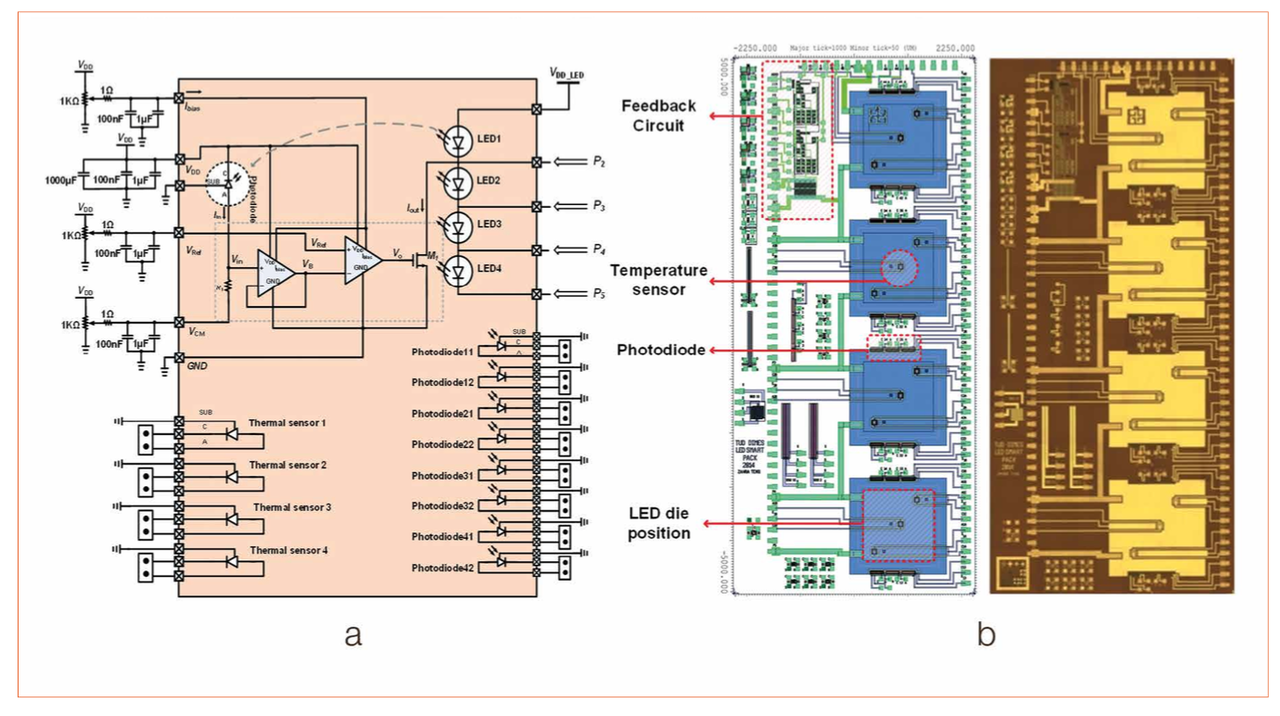 Figure 6: Schematic of the package (a) and layout and chip micrograph (b) showing component positions in the package
New challenges were emerged by moving from 2D SiP to a 3D package. In this case, a KOH etched cavity in Si interposer makes a high topography that brings up new challenges. It acts as a precision cavity with aluminum coating in place of sidewall mirror. The main challenge is the lithography aspect-ration with steps over a few hundred micrometers topography.
To overcome the conventional lithography limitations over high topographies, a high aspect ratio (HAR) lithography approach was developed that can be used both
for the 3D SiP and, in general, for litho-defined lateral wire bonding. Litho-defined wire bonding uses conventional CMOS interconnect toolset and processes in combination with multi-level lithography aiming for “wire bond like” interconnect structures and HAR interconnects. It also enables advanced heterogeneous integration of different components with less reliability issues and problems. This method consists of placing and attaching the chips on supporting substrate, passivation layer deposition, metal deposition and patterning through advanced high aspect ratio.
(3D) Lithography, which is the main key for such a method [20]. This method can be applied for heterogeneous integration areas, where a reliable and flexible interconnection method is critical.
Finally, a 3D silicon interposer was designed and fabricated for smart wafer level packaging of phosphor based white LED modules. It integrates different planar control blocks in addition to an on chip active reflector cup, which can improve light output efficiency of the package. The cup is implemented with a 200 μm KOH cavity coated later with a thin aluminum layer to form a mirroring sidewall. Furthermore, temperature and light sensors were fabricated on the cavity bottom and sidewall, respectively. The wires for LED driving current and sensor connections were patterned the whole way from top surface to cavity bottom. The fabrication process was the modified BiCMOS7 with 2 μm gate length. This new process enables to integrate different sensors and transistors on the top plane, cavity sidewall, and bottom. It also provides integration of large area LED chips with other functional devices. Different sensors were characterized. The bottom temperature sensor showed linear behavior of forward voltage versus package temperature at a constant forward bias current. The sidewall photodiodes with multi-stripe anode demonstrated a high responsivity to the emitted light. This is for the first time that a functional active device is fabricated on the sidewall of a silicon cavity.
The suggested smart Si-based interposer is not only applicable for LED WLP, but for a broad range of applications especially the ones with large area devices. It can monolithically integrate different performance monitoring and controlling blocks, in a low cost/area process line, which make a smart interface for the main device.
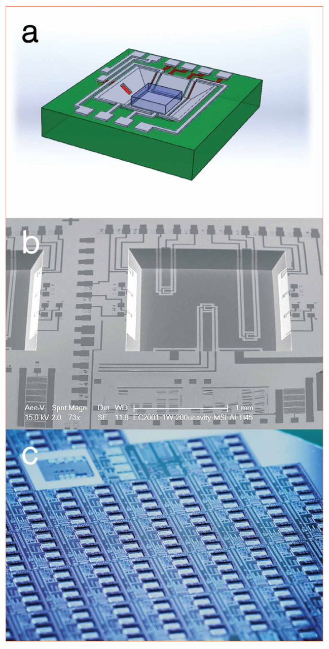 Figure 7: Unit cell of a 3D LED WLP, LED chip is mounted on an active reflector cup including sidewall light sensor, bottom temperature sensor and high aspect ratio litho defined wiring lines (a), SEM image of an active cavity including bottom and sidewall sensors, controlling blocks on top and litho-defined wiring (b), and photograph of a wafer level integration of 3D Si based interposer for Smart LED SiP (c)
Conclusion
Taking part in this tremendous developing industry and market demands, wafer level packaging can be considered as a key processing point. At present, most LED components are made with single chip packaging technology. The main manufacturing processes follow conventional chip-based IC packaging. So there is a need for LEDs to migrate to wafer level packaging to use the same benefits as IC’s. Hybrid integration of LED chips on a Si interposer can reduce the cost, and moreover, eases the integration of various functional devices. Using Si devices and capabilities makes it possible to design and fabricate a smart lighting module as a SiP for broad applications, especially in the Internet of Things (IoT) area. As IoT promises application diversification, the spotlight is now turned to advanced packages in order to answer market demands.
References:
[1] Y.-C. Lin, J. P. You, N. T. Tran, Y. He, and F. G. Shi, “Packaging of Phosphor Based High Power White LEDs: Effects of Phosphor Concentration and Packaging Configuration,” J. Electron. Packag., vol. 133, no. 1, p. 11009, 2011.
[2] H. Luo, J. K. Kim, E. F. Schubert, J. Cho, C. Sone, and Y. Park, “Analysis of high-power packages for phosphor-based white-light-emitting diodes,” Appl. Phys. Lett., vol. 86, pp. 1–3, 2005.
[3] J. K. Kim, H. Luo, E. F. Schubert, J. Cho, C. Sone, and Y. Park, “Strongly enhanced phosphor efficiency in GaInN white light-emitting diodes using remote phosphor configuration and diffuse reflector cup,” Japanese J. Appl. Physics, Part 2 Lett., vol. 44, no. 20–23, pp. 649–651, 2005.
[4] S. Chhajed, Y. Xi, Y. L. Li, T. Gessmann, and E. F. Schubert, “Influence of junction temperature on chromaticity and color-rendering properties of trichromatic white-light sources based on light-emitting diodes,” J. Appl. Phys., vol. 97, no. 5, pp. 1–8, 2005.
[5] H. Chen, A. Keppens, P. Hanselaer, Y. Lu, Y. Gao, R. Zhuang, and Z. Chen, “Failure analysis of electrical-thermal-optical characteristics of LEDs based on AlGaInP and InGaN/GaN,” Semiconductors, vol. 46, no. 10, pp. 1333–1338, 2012.
[6] J. K. Kim and H. C. Lee, “A photo-sensor on thin polysilicon membrane embedded in wafer level package LED,” in Proceedings of the SPIE, 2012, vol. 8431, pp. 8431–7.
[7] Z. Kolahdouz, A. Rostamian, M. Kolahdouz, T. Ma, H. van Zeijl, and K. Zhang, “Output blue light evaluation for phosphor based smart white LED wafer level packages,” Opt. Express, vol. 24, no. 4, pp. 174–177, 2016.
[8] R. Zhang, S. W. R. Lee, D. G. Xiao, and H. Chen, “LED Packaging using Silicon Substrate with Cavities for Phosphor Printing and Copper- filled TSVs for 3D Interconnection,” in Electronic Components and Technology Conference, 2011, pp. 1616–1621.
[9] C. T. Tsou and Y.-S. Huang, “Silicon-Based Packaging Platform for Light-Emitting Diode,” IEEE Trans. Adv. Packag., vol. 29, no. 3, pp. 607–614, Aug. 2006.
[10]W. K. Jeung, S. H. Shin, S. Y. Hong, S. M. Choi, S. Yi, Y. B. Yoon, H. J. Kim, S. J. Lee, and K. Y. Park, “Silicon-Based, Multi-Chip LED Package,” in 2007 Proceedings 57th Electronic Components and Technology Conference, 2007, pp. 722–727.
[11] L. Di Benedetto, M. Kolahdouz, B. G. Malm, M. Ostling, and H. H. Radamson, “Strain balance approach for optimized signal-to-noise ratio in SiGe quantum well bolometers,” in Solid State Device Research Conference, 2009. ESSDERC’09. Proceedings of the European, 2009, pp. 101–104.
[12] J. Y. Andersson, P. Ericsson, H. H. Radamson, S. G. E. Wissmar, and M. Kolahdouz, “SiGe/Si quantum structures as a thermistor material for low cost IR microbolometer focal plane arrays,” Solid. State. Electron., vol. 60, no. 1, pp. 100–104, 2011.
[13] H. H. Radamson and L. Thylén, Monolithic Nanoscale Photonics–Electronics Integration in Silicon and Other Group IV Elements. Elsevier Science & Technology, 2014.
[14] S. Chang and C. Tsou, “A Novel Silicon-Based LED Packaging Module With an Integrated Temperature Sensor,” IEEE Trans. Components, Packag. Manuf. Technol., vol. 4, no. 5, pp. 769–776, 2014.
[15]S. Y. Ron Hui, S. N. Li, X. H. Tao, W. Chen, and W. M. Ng, “A novel passive offline LED driver with long lifetime,” IEEE Trans. Power Electron., vol. 25, no. 10, pp. 2665–2672, 2010.
[16] K. Tseng and C. Tsou, “Novel silicon-based led packaging module with an integrated photosensing element,” IEEE Photonics Technol. Lett., vol. 25, no. 5, pp. 515–518, 2013.
[17] Z. Kolahdouz, PhD thesis, “Monolithic 3D Wafer Level Integration: Applied for Smart LED Wafer Level Packaging,” Delft University of Technology, ISBN: 978-94-028-0513-0, 2017.
[18] Z. Kolahdouz, M. Tohidian, H. Van Zeijl, M. Kolahdouz, and G. Q. Zhang, “Monolithically Integrated Light Feedback Control Circuit for Blue / UV LED Smart Package,” IEEE Photonics J., vol. 9, no. 2, 2017.
[19] Z. Kolahdouz Esfahani, A. Rostamian, M. Kolahdouz, T. Ma, H. Van Zeijl, and G. Q. Zhang, “Blue Selective Photodiodes for Optical Feedback in LED Wafer Level Packages,” in ESSDERC, 2014, pp. 174–177.
[20]Z. Kolahdouz Esfahani, H. Van Zeijl, and G. Q. Zhang, “High Aspect Ratio Lithography for Litho-Defined Wire Bonding,” in ECTC, 2014, pp. 1556–1561.
(c) Luger Research e.U. - 2017

