Status of Micro- and Nanostructured 3D LED Technologies
Conventional LEDs are planar, two-dimensional (2D) devices that emit light from a thin material layer at or near their flat surface. The vast majority of LEDs are made of GaN and InGaN material requiring expensive substrate wafers made of sapphire, silicon carbide or gallium nitride. The 3D WireLED technology uses silicon wafers for wafer diameters of 8 inches or larger. On each wafer, millions of vertical microwires and microrods of GaN are grown, each with a diameter of less than one micron. Mr. Arno Grabher-Meyer and Mr. Siegfried Luger from LED professional, talked with the General Manager of Aledia, Mr. Giorgio Anania about the status of this innovative technology.
LED professional: Before we go into details, can you tell us what the principle structure and performance of your 3D technology is?
Giorgio Anania: We are still developing these products so there are still unknowns related to performance. We are working with Gallium-Nitride with an m-plane instead of c-plane growth so we are in a different plane structure. However, the rest uses Gallium-Nitride. The fact that we have the quantum-wells wrapped in cylinders around the micro-wires, so co-cylindrical, makes the differences in the way the light is emitted - but the physics is the same as for m-plane, flat Gallium-Nitride.
LED professional: Let’s go back to the basic idea for the technology. What were the problems you were trying to overcome with the 3D technology?
Giorgio Anania: The basic argument is as follows: The industry has basically dropped the price of lumens per dollar by increasing the lumens or, let’s say, the efficiency. That starts getting flatter as the time moves on. Today, the approach used by the optics world is not made for high-volume, so it’s expensive. In order to address the cost issue, there’s no point in starting up with a 5% better solution than some of the Asian giants. We must think of an approach that is completely different; an approach with different characteristics. With microwires we can completely disconnect the light-emission, which can be a perfect micro wire crystal, from the substrate, just to be used as a carrier. The point is, you can disconnect the microwires from the substrates so you get a cheap substrate and and also have a large amount of substrate for mass production. In the 2-D world you will not get big cost savings by using GaN on Silicon instead of GaN on sapphire. The main advantage is that you can use the silicon CMOS foundaries. But you don’t get big cost savings because you still have over stresses related to putting the GaN coating on. If you put a big GaN buffer layer on silicon, which has to be thicker than on sapphire, it requires longer process times in the reactors. But the stress in the material still remains and this is exactly the point where the 3D concept shows the big advantages; especially when we build up the microwires on silicon instead of a separate GaN buffer layer.
 Figure 1: Nanowires are the basis of the 3D LED technology that promises several advantages over the conventional LED technology
LED professional: How large can the wafer sizes be with your technology and what other factors are related to the cost side?
Giorgio Anania: We can start at 8 inches because it’s cheap. Since most of the fabs in microelectronics moved from 8 to 12 inches, the remaining 8 inch fabs are offering lower prices. As soon as 12 inch wafer production gets cheaper we will move to 12 inches as well. The 3D LED technology with microwires and without any GaN buffer is completely scaleable in terms of wafer sizes. The breakthrough of this technology is really that the emitting crystal is stress free even when processing big wafer sizes. Our 3D technology is not just a silicon based LED because microwires have a much lower material content than the GaN buffer layer, it’s the throughput which is very fast through the MOCVD machine and the fact that you can use generally available plants and that you can have more surface area.
LED professional: There are a lot of arguments for 3D micro wire technology, costwise. What about the performance figures?
Giorgio Anania: There are some non-cost advantages you can get which are quite significant. For example, a 1 mm2 2D LED chip will have approximately 1 mm2 of emitting area. Theoretically, with the micro wire technology you have the potential to increase surface area - in other words you’ll get more light out of an 3D 1 mm2 LED chip compared to the 2D technology.
LED professional: Are there limits in the lengths of the microwires? How far forward can this technology go?
Giorgio Anania: It’s a trade-off. The more concentrated they are and the taller they are the more surface area you have. But you also have more difficulties in extracting light. The farther away they are, the much more light output you’ll get. But you lose surface area. So the question is, where’s the optimum?
LED professional: Would it be possible to get the same amount of light out of a smaller LED die? This would be especially advantageous for applications like spotlighting!
Giorgio Anania: There are some markets that are very sensitive to that. Automotive applications that are looking for higher brightness are an example. Here it’s important to get more light from the same surface.
LED professional: What about colored light or CCT tunable light?
Giorgio Anania: In 2D the shift to red is done with indium. But the amount of indium is limited with the 2D technology. So you can’t get GaN emitting in the red. For this, you have to go to other materials. In the case of microwires and nanowires there’s the possibility to put in more indium with all the possibilities of having GaN emitting in blue, yellow, green or red. With 2D you just do the blue and combine it with the phosphors.
LED professional: Is this process done on a wafer level or on a microwire level?
Giorgio Anania: One nanowire could have 10% indium and it emits yellow whereas another one has 20% indium and emits orange. The question is; how can you have a certain number of nanowires absorbing 20% of the indium and other nanowires absorbing 15% and yet another set of nanowires absorbing 20% of the indium on one chip giving you the distribution that you want, so you can simulate a black body emission, for example?
With 2D the doping determines the emission and you don’t have a lot of possibilities to change the blue. With 3D you can actually generate a different population of colors on the same LED die. This new feature is not our first target because we want to deliver a low-cost solution first. Once we get the blue under control we will work on the colors. LED technology (left) and the 3D microwire technology (right)") Figure 2: Comparison of the conventional 2D (planar) LED technology (left) and the 3D microwire technology (right).
Figure 2: Comparison of the conventional 2D (planar) LED technology (left) and the 3D microwire technology (right).
2D LEDs:
- Small, expensive substrate
- Slow MOCVD growth process (high capital expenditure)
- High materials consumption
- LED-specific manufacturing plants
- Light emission area = at most the 2D area
- Single color on one wafer
3D LEDs:
- Large, economical substrate
- Fast MOCVD growth process (low capital expenditure)
- Low materials consumption
- Existing high-volume silicon wafer fabs
- Light emission area = up to 3x the 2D area = more light/mm2 or less current density, less efficiency droop
- Multiple colors on one wafer or even on one chip
LED professional: How about the market roadmap for this 3D technology?
Giorgio Anania: The prototypes will be available at the beginning of next year. The first products will be qualified in the second half of 2014 and will be available in 2015.
LED professional: What kind of product levels will you offer?
Giorgio Anania: We will sell packaged LEDs. We will do the nanowires growth inside and organize packaging with subcontractors. We are looking fortraditional packaging approaches “me-too” would be available at a lower cost. We also have a lot more opportunities when processing 8 or 12-inch wafers.
LED professional: Do you have plans for licensing your technology to others?
Giorgio Anania: You cross the road when you get there. The basic structure of our company is a manufacturing entity not a licensing entity. Of course there are some markets where one player owns 90% of the world market then you may decide do a licensing deal but those are things you can only decide when the time comes. The general strategy of our company is that of an industrial manufacturing company.
LED professional: What are the critical things you are working on to get your technology right for the market?
Giorgio Anania: Our objective is to target large commodity markets. In this market you want to go with the largest customers and do a deal with them. It’s different to go through distribution networks with a vast numbers of specifiers. When it’s a commodity the price is the main thing. The 3D technology does have more parameters then the 2D technology. So it’s not an easy task to optimize those. Anyone can play around and show some good results with microwires. But to really optimize for high-volume and high-efficiency you need hundreds and hundreds of wafer-runs. There are no technology blockages or limitations such as current density, light extraction, thermal dissipation etcetera.
LED professional: What about your global position with microwire or nanowire LED technology approaches?
Giorgio Anania: There are some other players. Our approach is probably unique because it’s focused very heavily on technical decisions that aim for low cost.
LED professional: Thank you for this interview and all the best with your innovative technology!
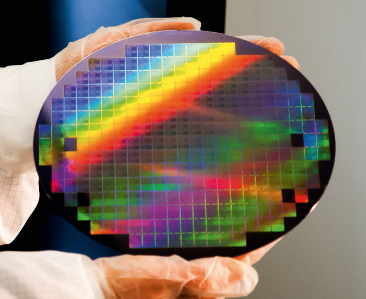
Giorgio Anania: Thank you. Figure 3: One of the major advantages of this 3D technology is that big Si-wafers like this 200mm wafer can be used and stress due to lattice mismatch is minimized
About Giorgio Anania
Giorgio Anania is co-founder, president and CEO. He has spent more than 30 years in senior management at high-technology companies, from start-up ventures to international public companies, and has led two successful IPOs. He is chairman of Cube Optics AG and vice president of the executive board at Photonics21. Previously, Giorgio was CEO of Bookham, now Oclaro, which he grew from a start-up into a quarter-billion-dollar NASDAQ-listed public company. He also served as the vice president of sales, finance and business development for Flamel Technologies. Prior to that, he was the founder and general manager of the Miniplex DSL Business Unit at Raychem and strategy consultant at Booz Allen. He has a M.A. degree in physics from Oxford University and a Ph.D. in thermonuclear fusion from Princeton University.
