Thin-Film Light Management System for Intelligent Large-Area LED Luminaires by the Centre Suisse d’Electronique et de Microtechnique SA
The recent advances in Solid State Lighting have triggered the development of smart lighting solutions. However, the point-like nature of LEDs imposes the use of inefficient and/or bulky light scattering sheets or costly, short-pitch LED arrays to achieve acceptable spatial luminance uniformity. Ph.D. Oscar Fernandez, Senior R&D Engineer at the Centre Suisse d’Electronique et de Microtechnique SA (CSEM) shows a new approach in the form of an innovative thin form-factor light management (LM) system comprising a highly engineered combination of thin-film diffractive nano-optical and refractive micro-optical elements.
The recent advances in the domain of Solid State Lighting (SSL) and, in particular, in Light Emitting Diode (LED) technology has triggered the development of smart lighting solutions. However, the point-like nature of the LEDs imposes the use of either inefficient and/ or bulky light scattering sheets or costly short-pitch LED arrays to achieve acceptable spatial luminance uniformity in, for example, large-area luminaires for professional lighting.
Here, we present an innovative thin form-factor light management (LM) system comprising a highly engineered combination of thin-film diffractive nano and refractive micro-optical elements. Our LM solution allows the decreasing of the LED pitch by a factor of 2-3, hence reducing the amount of LEDs for a given total emitting area and luminous flux.
The accurate prediction of the system optical response is achieved using interfaced rigorous and ray-tracing modelling tools. Such interfacing is fundamental to account for the complex optical interplay of the different components in the system and, therefore, to ensure meaningful simulation results. The optimized system demonstrates excellent efficiency and luminance spatial uniformity even when combined with long-pitch LED arrays.
The LM system presented here has been developed in the framework of the EU-funded project, LASSIE-FP7, whose objective is the realization of a cost-efficient, large-area, efficient, intelligent luminaire with outstanding light quality.
Introduction
Lighting represents almost 20% of global electricity consumption [1], similar to the amount of electricity generated by nuclear power and equivalent to 70% of the emissions from the world’s light passenger vehicles. The development and implementation of more efficient lighting systems will undoubtedly make a significant contribution to controlling global CO2 emissions. In addition, LEDs do not contain mercury, in contrast to high efficiency fluorescent lamps.
The high efficacy values, close to 60% for commercially available high-power blue and well over 120 lm/W for commercial cool white LEDs, achieved in the last years together with standard lifetime values in excess of 50,000 hours under continuous operation makes LEDs the most convenient light source for energy savings. In fact, LED technology is expected to conquer the lighting market in the coming years with a penetration rate of 56% by 2016 [2].
Large-area light sources represent the most convenient option when a large amount of light is needed and are, therefore, widely used in a variety of lighting segments including office, shop-retail, hospitality, industrial and architectural lighting segments, which are predicted to be worth 40 billion Euros in 2020 [3].
Organic light-emitting diodes (OLEDs), the organic counterparts of LEDs are flat, thin, surface emitting devices that have been seen as the “next big thing” in large-area lighting and the natural successors of LEDs for large-area products. However, several factors exist that are causing OLEDs to struggle on their way to the general lighting market and that, according to many, will likely prevent this ever happening.
On the one hand, OLED technology lags well behind LED in terms of efficacy, lifetime, lumen output and lumen-per-dollar. Indeed, the ever promised large-area, low-cost, solution-based R2R fabrication on flexible substrates is not even close to becoming a reality in the next years. On the contrary, commercially available OLEDs today are expensive, glass-based devices, manufactured using several expensive evaporation processes under vacuum in a sheet-to-sheet process and with emissive areas of typically 100 cm2 or less (Table 1).
") Table 1: Performance comparison of current best commercially available OLEDs and standard LED-based large-area lighting modules (effective summer 2015)
Table 1: Performance comparison of current best commercially available OLEDs and standard LED-based large-area lighting modules (effective summer 2015)
Please Note:
1 Including thermal back plate, housing and wiring; 2 at 340 mA and 19 V; 3 at 300 lumen ; 4 4000 K planned; 5 at 300 lumen; 6 at 125 lumen; 7 for orders above 40 OLEDs (http://www.oled-info.com/philips-launches-new-sales-campaign-sees-oleds-reaching-mass-market-early-2017); 8 bare OLED; 9 1700 mA, 8.5 V; 10 at 3000 cd/m2; 11 using LG proprietary “Face Seal” technology; 12 with housing and wiring; 13 initial luminance not specified; 14 https://www.maritex.com.pl/en/oled-lg-chem-lighting/olp-n8sa30-i-34063-c-33634; 15 http://www.oled-info.com/lg-details-price-their-320x320-mm-and-truly-flexible-oled-lighting-panels; 16 not quoted for the lamp, given figure is based on the lifetime information of the LED chips; 17 http://www.futurelightingsolutions.com/en/Technologies/ Semiconductors/Lighting-Solutions/LED-Light-Modules/Pages/3029132-LLFML66-38K308A.aspx?ManufacturerName=LG-INNOTEK&isFLS=true&IM=0
On the other hand, non-transparent, scattering out-coupling films used to boost device efficacy and to alleviate cavity-related angular color shift, are not compatible with appealing mirror-like or transparent off-state appearance, a many-times cited advantage of OLED technology.
Finally, most of the mentioned unique selling points of OLED technology such as large-area, low-cost, transparency and flexibility have continuously been eroded by LED-based technology. In fact, large-area, 600 x 600 mm2, luminaires based on LEDs have been available on the market for a few years.
A common approach is to eliminate the hot spots associated with the LEDs by using a diffusing plate located a certain distance from the light sources. Regardless of its simplicity, uniform luminance completely free of appreciable hot-spots, requires a distance of a few centimetres between the LEDs and the diffuser, an approach incompatible with thin form-factors and/or device flexibility. Although diffusers with large hiding factors can be used in closer proximity to the sources, it comes at a substantial drop in efficacy as shown in figure 1.
 for diffusing plates based on volumetric scattering manufactured by Bayer; modified from [4]")
Figure 1: Optical transmittance versus half power angle (hiding power) for diffusing plates based on volumetric scattering manufactured by Bayer; modified from [4]
A way to overcome this issue is the so-called edge-lit technology where the LEDs are distributed across at least one of the edges of a thin transparent plate. The light emitted by the LEDs is coupled inside the waveguide and guided through total internal reflection (TIR). Light extraction features replicated on the emissive surface/s of the waveguide disturb the TIR and allow the guided light to escape.
In large-area edge-lit luminaires, a large part of the emitted light has to be guided across long distances, which results in high optical losses even when relatively transparent materials such as PMMA are used (PMMA absorption coefficient of 0.0017 mm-1 [5] leads to 17% optical losses on a 100 mm length). In addition, since the waveguide perimeter increases only as the square root of its area, high LED densities are required as the emissive area increases which demand efficient thermal management solutions to avoid excessive heat at the waveguide edges to prevent associated detrimental effects such as waveguide deformation and/or material yellowing.
A different approach consists in embedding white LEDs inside the waveguide, evenly distributed across its area [6]. This technology solves some, but not all the issues related to edge-lit. For example, moderate-to-high temperatures around the LEDs over sufficiently long time periods may degrade the waveguide material locally close to the LEDs. Therefore, unless an expensive, short-pitch LED configuration is adopted, the maximum attainable brightness of the luminaire is noticeably limited. Also, non-standard side-emitting LEDs or precisely tilted standard surface-emitting LEDs are required as otherwise most of the light will leave the waveguide without undergoing TIR, giving rise to appreciable hot-spots. Moreover, as the LEDs must be fully embedded into the waveguide, a minimum thickness of the latter is mandatory.
Our light management technology (patent pending) was designed and engineered to overcome the mentioned shortcomings. It is based on the use of diffractive elements and blue LEDs. By using diffractive nanostructures, light emitted around the normal to the LED surface can be efficiently in-coupled even for standard, surface-emitting, LEDs located outside the waveguide. The spatial separation of light emission and light guiding/ out-coupling results in a minimum temperature-driven degradation effect in the waveguide material and allows the use of much thinner waveguides.
White LED emission can be achieved using the so-called multichannel or RGB approach. This approach uses a combination of red, green and blue LEDs (often 4 or 5 different “colors” are used). When appropriately driven, such combination produces a white light of a predetermined correlated temperature (CCT). Although compatible with CCT tuning, it suffers from low efficacy values at medium to low CCT values due to the low efficacy of green/ amber LEDs in the so-called green gap. In addition, the spectral distribution of the resulting white light, formed by the superposition of few relatively narrow spectra, results in a substantial number of missing wavelengths and the consequent color misinterpretation, (poor color rendition) of objects with emittances around these wavelengths. Finally, the differential aging of the red, green and blue LEDs must be properly compensated to avoid undesired CCT shift during device operation.
Alternatively, in the so-called phosphor approach, a layer of a yellow phosphor-containing resin is deposited on top of a blue LED chip. Part of the blue light passing through the phosphor layer experiences Stokes down-conversion, resulting in a white emission whose CCT is determined by the composition of the phosphor layer and its thickness.
Phosphor-containing white LEDs give a much broader emission spectrum than CCT-equivalent RGB LEDs and hence better color rendition. In fact, CRI values as high as 98 have been reported using a combination of green, yellow and red phosphors [7] [8]. Moreover, with phosphors near to 100% quantum yields, phosphor white LEDs are also more efficient than RGB.
However, the phosphor approach also suffers from CCT shift and efficiency drop related to the wavelength shift of the pumping blue LEDs during operation and, more importantly, to the phosphor degradation and emission quenching observed primarily at high temperatures. For example, a 10% drop in down-conversion quantum efficiency or in the phosphor absorption coefficient (in the blue region) can cause a color shift close to a MacAdam ellipse step size 4 [9]. High temperatures also cause local delamination of the phosphor layer form the LED surface which results in a noticeable CCT shift [10]. These temperature-driven detrimental effects can be highly alleviated by locating the phosphor layer away from the emitting chip in what is known as remote phosphor approach.
Thin-Film Light Management Foil
Contrary to the continuous improvements in LED efficacy and optical power output, the secondary optics of large-area LED-based luminaires has not improved much [11]. Indeed, as mentioned earlier, today’s large-area LED luminaires, the spatial and angular distribution of the light emitted by the individual LEDs, is still controlled by thick volumetric scattering plates, distant thin-film diffusers in combination with reflectors and/or refractors which results in bulky and heavy luminaires. Thin and light LED-based luminaires require alternative technologies.
Figure 2: Comparison of an LED array with a PC foil. The left image shows a misalignment of the gratings and the LED while the right image shows well-aligned, in-coupling diffractive elements
Light in-coupling
In our solution, the light emitted by blue LEDs is in-coupling into a thin-film, flexible transparent waveguide through diffractive in-coupling elements replicated on the largest surface of the waveguide. The in-coupling diffractive elements are replicated in the form of pixels and distributed across the waveguide following the same pattern as the LEDs in the substrate. Each in-coupling pixel covers an area similar to that of the LEDs. When the waveguide is located at close distance from the LEDs and the in-coupling pixels aligned with respect to the sources, a substantial amount of the emitted light is in-coupled inside the waveguide.
This approach has the following advantages with respect to other approaches mentioned above:
- The decoupling of the light in-coupling from the waveguide edge allows using much thinner waveguides with the immediate reduction in weight and cost. In addition, the increased flexibility of the waveguide opens the door for Roll-to-Roll manufacturing
- The increased in-coupling area is compatible with higher LED density with still manageable integration of heat management solutions
- The regular spatial distribution of the LEDs over the emissive area results in shorter light travel distances and hence, in lower optical losses in the waveguide
- The physical separation between the LED (i.e. heat) sources and the waveguide ensures the mechanical and optical integrity of the waveguide during device operation
- High in-coupling efficiency values of 50% have been theoretically predicted for optimized in-couplers in combination with lambertian blue LEDs. Higher values are expected when additional diffractive in-couplers are added on the top surface of the waveguide. Moreover, in-coupling efficiency values in excess of 80% are expected for polar incident angles between -10 and 10° with respect to the normal (Figure 3)

Figure 3: In-coupling efficiency plotted as a function of the polar incident angle for 0° azimuthal incident angle
Figure 2 shows an array of pixelated in-coupling gratings replicated on a 0.5 mm thick PC foil located on top of a LED board (manufactured by VTT) comprising a 3 x 3 array of blue LEDs. On the left image no light in-coupling observed due to the misalignment of the gratings and the LEDs. On the right image a part of the light emitted by the LEDs is in-coupled into the waveguide by the well-aligned in-coupling diffractive elements.
In addition, each of such in-coupling pixels contains a series of 100 x 100 μm linear 1-dimensional gratings with optimum grating parameters with their grooves oriented in two perpendicular directions in a chessboard arrangement which ensures light in-coupling in two in-plane directions as shown in figure 4.
 in two in-plane perpendicular directions as described in the article")
Figure 4: Light in-coupling (and subsequent out-coupling) in two in-plane perpendicular directions as described in the article
Light out-coupling
The in-coupled light travels inside the waveguide based on total internal reflection, TIR, at the interface between the top surface of the waveguide and air. The TIR condition is disrupted by the presence of out-coupling structures allowing the in-coupled light to escape the waveguide.
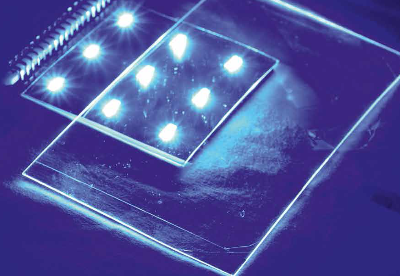
For light out-coupling, our approach uses out-coupling pixels of similar size to the in-coupling pixels. They can be replicated on the top and/or the bottom surface of the waveguide and can comprise diffractive nano- (Figure 5) or refractive microstructures (Figure 6).

Figure 5: Comparison of a 3 x 3 LED array without and with LM foil
The left image of figure 5 shows a 50 x 50 mm2 LED board with a 3 x 3 LED array fabricated by VTT. The right picture shows the same LED board an LM foil with a 3 x 3 array of in-coupling pixels aligned with respect to the LEDs and 16 out-coupling pixels; light in- and out-coupling is observed. A considerable amount of in-coupled light remains trapped and partially leaves the waveguide through its edges due to the relatively low out-coupling efficiency.
Figure 6 shows a light, edge-coupled into a 0.5 mm thick PC foil. In the left image, the light propagates via TIR through the waveguide and leaves primarily at the opposite edge. In the right image, the replicated microstructures disturb the TIR and force the light to be coupled out the waveguide; the light emitted through the opposite edge is negligible, indicative of high out-coupling efficiency.
This way, the light emitted by the LEDs is spread inside the waveguide and coupled-out towards the viewer.

Figure 6: Light edge-coupled into a 0.5 mm thick PC foil
Color conversion
The out-coupled blue light is down-converted using BASF (Ludwigshafen, Germany) proprietary thin-film color changing films (CCF) remotely located with respect to the LED sources. By carefully engineering (for a given blue light source) the chemical composition of the individual dyes and their combination in the film, white light with a color of different CCTs along the Planckian locus can be produced. BASF CCFs contain organic phosphors that, due to the unresolved molecular vibrational levels, render a broad emission spectrum, which, in turn, results in high color rendering index (Table 2).
 and two different CCFs from BASF")
Table 2: Photometric data of the down-converted white light using an array of blue LEDs (lmax= 460 nm) and two different CCFs from BASF
In addition, by carefully engineering the chemical composition of the individual dyes, their combination in the foil and the binding material, high efficacy and long lifetime has been demonstrated.
Conclusions
A new approach has been presented for the fabrication of thin-film efficient LED-based lighting modules compatible with R2R production. This approach has demonstrated the potential to overcome the fundamental limitations of current technologies for the fabrication of efficient thin-film lighting modules with high luminance uniformity and excellent spectral properties with a reduced number of LEDs.

Figure 7: CIE1976 u’v’ coordinates of the down-converted white light using two different CCFs from BASF in combination with a blue light of max 460 nm
Acknowledgements:
The authors would like to thank S. Ivanovici at BASF (Ludwigshafen, Germany) for the supply of the Color Changing Films, B. Koller at REGENT LIGHTING AG (Basel, Switzerland) for the measurement of the white devices and Kimmo Keränen and Olli Tapaninen at VTT (Oulu, Finland) for the supply of the blue LED substrates.
The research leading to these results has received funding from the European Union Seventh Framework Programme [FP7/2007-2013] under grant agreement n°619556, project LASSIE-FP7.
References:
[1] http://www.photonics21.org/download/SRA_2010.pdf
[2] A. Prasad, “2015 Year of (LED) Light”, LED Professional 47, pp. 32-36 (2015)
[3] Lighting the way: Perspectives on the global lighting market, 2nd Edition, McKinsey and Company (2012)
[4] www.plastics.bayer.com/~/media/Product%20Center/PCS/Images/5_Library/Broschueren/ LED%20Brochure/ MS00069823_LED-Brosch.ashx
[5] J-P. Lauret, “Selecting the Ideal Material for Improved Optical Solutions”, Proc. LpS2014 pp. 228-237.
[6] J. Gourlay, “Making Light Work - Light Sources for Modern Lighting Requirements”, LED Professional, 47 (2015) pp. 72-75
[7] J. Carey, ”Intematix expands phosphor development and IP to meet demanding SSL applications”, LEDs Magazine, March 2014, pp.21-25
[8] R. Mueller-Mach, G. Mueller, M.R. Krames, H.A. Höppe, F. Stadler, W. Schnick, T. Juestel and P. Schmidt, “Highly efficient all-nitride phosphor-converted white light emitting diode”, Physica Status Solidi (a), 202 (9), pp. 1727-1732 (2005)
[9] C. Sommer, P. Hartmann, P. Pachler, H. Hoschopf, F.P. Wenzl, “White light quality of phosphor converted light-emitting diodes: A phosphor materials perspective of view”, J. Alloys Comp. 520 pp. 146-152 (2012)
[10] R.C. Tuttle, “Method for Projecting Color Shift of High-Power LED Package”, Proc. LpS2014, pp. 46-54.
[11] M. Macha, “Optomechanical Nanostructures for Overcoming Fundamentals in Optics Design”, Proc. LpS2014, pp-214-219
