External extraction light emitting diode based upon crystallographic faceted surfaces
A light emitting diode is disclosed that includes a support structure and a Group III nitride light emitting active structure mesa on the support structure. The mesa has its sidewalls along an indexed crystal plane of the Group III nitride. A method of forming the diode is also disclosed that includes the steps of removing a substrate from a Group III nitride light emitting structure that includes a sub-mount structure on the Group III nitride light emitting structure opposite the substrate, and thereafter etching the surface of the Group III nitride from which the substrate has been removed with an anisotropic etch to develop crystal facets on the surface in which the facets are along an index plane of the Group III nitride. The method can also include etching the light emitting structure with an anisotropic etch to form a mesa with edges along an index plane of the Group III nitride.


Background of the invention
[0002] The present invention relates to light emitting diodes (LEDs) formed in wide bandgap materials and in particular relates to improving the extraction of light from such LEDs.
[0003] A light emitting diode is a semiconductor photonic device that emits light upon the recombination of electrons and holes in the semiconductor material or material system. The recombination is typically driven by a voltage bias across p-type and n-type materials that form a p-n junction. Because the recombination is a quantum mechanical step, the photon generated, its energy, and thus the frequency and wavelength (perceived as color) of the photon will depend upon the maximum energy of a permitted recombination transaction.
[0004] The visible colors green, blue, and violet, along with the ultraviolet portion of the electromagnetic spectrum, represent higher frequencies and thus higher energy photons. As a result, blue light can only be produced by materials with bandgaps of at least about 2.6 electron volts (eV). In turn, because blue is a primary color and is particularly desirable for full-color devices and devices that produce white light (as a combination of red, green, and blue), much recent interest has focused upon improvements in wide bandgap light emitting diodes form from materials such as silicon carbide, diamond, and the Group III nitrides. In particular, light emitting diodes formed of Group III nitride active regions continue to gain increasing commercial acceptance and are becoming more common in everyday applications.
[0005] A number of factors taken together produce the visible emission of a light emitting diode. As a potential limiting factor, however, not every recombination-generated photon externally exits the physical diode. Stated differently, a given voltage will produce a given number of recombination events which will in turn generate a given number of photons (not necessarily the same number). Not all of the generated photons, however, will be externally emitted as visible light. Instead, the photons are subject to competing factors including reabsorption and internal reflection. Accordingly, all other factors being equal, one goal for increasing the visible output of a light emitting diode is to increase the fraction (percentage, proportion) of photons that physically escape the diode in an intended illuminating direction.
[0006] The effect of Snell's law represents another factor in the external emission of an LED; i.e., the behavior of light as it meets an interface between two different materials. Specifically, when light waves reach such an interface, they will either reflect or refract. The difference (as well as any angle of refraction) depends upon the index of refraction of the adjacent material and the incident angle of the light. In an LED, one of the adjacent materials is a semiconductor and the other is the bordering environment. In some cases this is air, while in other cases it is a lens material, frequently a polymer transparent to frequencies within the visible range. Increasing the number of different angles at which emitted photons meet the boundary correspondingly increases the statistical probability that more photons will be emitted, rather than internally reflected. Accordingly, as the electronic efficiency of Group III nitride based diodes has increased, opportunities to increase efficiency based on the boundary have become more attractive. Examples of these efforts include (but are not limited to) U.S. Pat. No. 6,791,119 and U.S. Patent Application Publication Nos. 20040041164 and 20050247950 which are commonly assigned with the present invention.
Brief summary of the invention
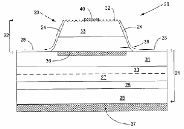
[0007] In one aspect the invention is a light emitting diode that includes a support structure and a Group III nitride light emitting active structure mesa on the support structure. The mesa has its sidewalls along an indexed crystal plane of the Group III nitride.
[0008] In another aspect, the invention is a method of forming a light emitting diode with improved light extraction. In this aspect the method includes the steps of removing a substrate from a Group III nitride light emitting structure that includes a sub-mount structure on the Group III nitride light emitting structure opposite the substrate, and thereafter etching the surface of the Group III nitride from which the substrate has been removed with an anisotropic etch to develop crystal facets on the surface in which the facets are along an index plane of the Group III nitride. The method can also include etching the light emitting structure with an anisotropic etch to form a mesa with edges along an index plane of the Group III nitride.
[0009] The foregoing and other objects and advantages of the invention and the manner in which the same are accomplished will become clearer based on the followed detailed description taken in conjunction with the accompanying drawings.
Claims
1. A light emitting diode comprising:
a Group III nitride light emitting active structure mesa;
said mesa having its sidewalls along an indexed crystal plane of the Group III nitride.
2. A light emitting diode according to claim 1 wherein the emitting face of said diode is a Group III nitride surface of said active structure. 3. A light emitting diode according to claim 1 further comprising a support structure for said mesa, said support structure being selected from the group consisting of metals, semiconductor substrates, and sub-mount structures. 4. A light emitting diode according to claim 1 wherein said light emitting active structure comprises at least one p-type layer of gallium nitride and at least one n-type layer of gallium nitride.
5. A light emitting diode according to claim 4 wherein said gallium nitride layers terminate in said indexed crystal plane edge of said mesa.
6. A light emitting diode according to claim 1 wherein said mesa sidewalls are along the (hkil) crystal plane of gallium nitride.
7. A light emitting diode according to claim 1 wherein said mesa sidewalls are along the {10-11} family of crystal planes of hexagonal gallium nitride.
8. A light emitting diode according to claim 1 further comprising a mirror between said light emitting active structure and said support structure.
9. A plurality of light emitting diodes according to claim 1 on a common wafer.
10. A light emitting diode according to claim 1 further comprising a roughened surface formed of a plurality of crystallographic features that demonstrate indexed planes of the Group III nitride.
11. A light emitting diode according to claim 10 wherein said indexed planes of said roughened surface are congruent with the indexed plane of said mesa sidewall.
12. A light emitting diode according to claim 1 comprising an ohmic contact to said support structure and an ohmic contact to said active structure.
13. A light emitting diode according to claim 10 comprising an ohmic contact to said roughened surface.
14. A light emitting diode according to claim 1 wherein said sidewalls form an angle of between about 58 and 62 degrees with respect to said support structure.
15. A light emitting diode according to claim 1 wherein said mesa has two part sidewalls, with a first major part along the indexed plane and a second major part at an obtuse angle with respect to said first part.
16. A method of forming a light emitting diode with improved light extraction, the method comprising:
anisotropicly etching the surface of a Group III nitride layer to develop crystal facets on the Group III nitride surface in which the facets are along an index plane of the Group III nitride.
17. A method according to claim 16 comprising removing a substrate from a Group III nitride light emitting structure that includes a sub-mount structure on the Group III nitride light emitting structure opposite the substrate prior to the anisotropic etching.
18. A method according to claim 16 comprising etching the light emitting structure with an anisotropic etch to form a mesa with edges along an index plane of the Group III nitride.
19. A method according to claim 18 comprising etching the mesa first and thereafter etching the Group III nitride surface to produce an indexed mesa sidewall, but without individual faceted features.
20. A method according to claim 18 comprising etching the Group III nitride surface first and thereafter etching the mesa sidewalls to produce index plane mesa sidewalls that include a plurality of individual index plane facets.
21. A method according to claim 18 comprising forming a plurality of mesas on a common wafer.
22. A method according to claim 21 comprising forming the mesas with the individual junctions between devices on the wafer are separated from one another by the anisotropic etch so that the layers that form the light emitting active structure terminate in the same indexed edge as the rest of the mesa.
23. A method according to claim 16 comprising removing a silicon carbide substrate from the Group III nitride light emitting mesa structure and thereafter etching the mesa structure to develop mesa sidewalls that are crystal facets along an index plane of the Group III nitride.
24. A method according to claim 23 comprising developing the mesa sidewalls along the same index plane as the mesa sidewalls.
25. A method according to claim 16 comprising removing the substrate from a gallium nitride light emitting structure.
26. A method according to claim 16 comprising etching the Group III nitride surface with an etchant selected from the group consisting of potassium hydroxide, sodium hydroxide, potassium hexacyanoferrate, and combinations thereof.
27. A method according to claim 18 comprising etching the mesa with an etchant selected from the group consisting of potassium hydroxide, sodium hydroxide, potassium hexacyanoferrate, and combinations thereof.
28. A method according to claim 16 further comprising dry etching at least a portion of the mesa sidewalls.
29. A method according to claim 28 comprising dry etching the mesa sidewalls before anisotropicly etching the sidewalls.
30. A method according to claim 28 comprising dry etching the mesa sidewalls after anisotropicly etching the sidewalls.
31. A light emitting diode with enhanced light extraction characteristics, comprising:
a sub-mounting structure;
at least one n-type and one p-type layer of Group III nitride on said sub-mounting structure and forming p-n junction for recombination of carriers and emission of photons under an applied voltage;
said group three nitride layers forming a mesa above said sub-mount structure in which the side walls of said mesa are defined by an indexed plane of said Group III nitride;
said diode terminating in one of said Group III nitride layers, with said terminal Group III nitride layer forming the light emitting surface of said diode;
said light emitting surface being formed of a plurality of crystal structures that demonstrate indexed planes of the Group III nitride;
an ohmic contact to said light emitting surface; and
an ohmic contact to said sub-mount structure.
32. A light emitting diode according to claim 31 further comprising a passivation layer on said mesa side walls and upper portions of said sub-mount structure for electrically isolating and environmentally protecting said Group III nitride layers in said mesa.
33. A light emitting diode according to claim 32 wherein said passivation layer is selected from the group consisting of silicon dioxide, stoichiometric silicon nitride, nonstoichiometric silicon nitride, and combinations thereof.
34. A light emitting diode according to claim 31 wherein said sub-mount structure comprises a plurality of metal and semiconductor layers that bond said Group III nitride layers to said sub-mount structure and that prevent undesired migration of dopants or other materials from the sub-mount structure to the Group III nitride layers.
35. A light emitting diode according to claim 31 further comprising a mirror layer between said sub-mount structure and said Group III nitride layers for enhancing the light extraction from said diode.
36. A light emitting diode according to claim 31 wherein said Group III nitride layers are selected from the group consisting of gallium nitride, aluminum gallium nitride, and aluminum indium gallium nitride.
37. A light emitting diode comprising a Group III nitride light emitting active structure mesa having chemically developed sidewalls.
38. A light emitting diode according to claim 37 wherein the emitting face of said diode is a Group III nitride surface of said active structure.
39. A light emitting diode according to claim 37 further compromising a support structure for said mesa, said support structure being selected from the group consisting of metals, semiconductor substrates, and sub-mount structures.
40. A light emitting diode according to claim 37 wherein said light emitting active structure comprises at least one p-type layer of gallium nitride and at least one n-type layer of gallium nitride.
41. A light emitting diode according to claim 40 wherein said gallium nitride layers terminate in said indexed crystal plane edge of said mesa.
42. A light emitting diode according to claim 37 wherein said mesa sidewalls are along the (hkil) crystal plane of gallium nitride.
43. A light emitting diode according to claim 37 wherein said mesa sidewalls are along the {10-11} family of crystal planes of hexagonal gallium nitride.
44. A light emitting diode according to claim 37 further comprising a mirror between said light emitting active structure and said support structure.
45. A plurality of light emitting diodes according to claim 33 on a common wafer.
46. A light emitting diode according to claim 37 further comprising a roughened surface formed of a plurality of crystallographic features that demonstrate indexed planes of the Group III nitride.
47. A light emitting diode according to claim 46 wherein said indexed planes of said roughened surface are congruent with the indexed plane of said mesa sidewall.
48. A light emitting diode according to claim 37 comprising an ohmic contact to said support structure and an ohmic contact to said active structure.
49. A light emitting diode according to claim 46 comprising an ohmic contact to said roughened surface.
50. A light emitting diode according to claim 37 wherein said sidewalls form an angle of between about 58 and 62 degrees with respect to said support structure.
51. A light emitting diode comprising:
a Group III nitride light emitting active structure mesa;
an emitting surface on said mesa formed of a plurality of crystallographic features and
said mesa having sidewalls geometrically congruent with said crystallographic features on said emitting surface.
52. A light emitting diode according to claim 51 further comprising a support structure for said mesa, said support structure being selected from the group consisting of metals, semiconductor substrates, and sub-mount structures.
53. A light emitting diode according to claim 51 wherein said light emitting active structure comprises at least one p-type layer of gallium nitride and at least one n-type layer of gallium nitride.
54. A light emitting diode according to claim 51 wherein said mesa sidewalls and said surface crystallographic features are along the (hkil) crysta55. A light emitting diode according to claim 51 wherein said mesa sidewalls are along the {10-11} family of crystal planes of hexagonal gallium nitride. 56. A plurality of light emitting diodes according to claim 51 on a common wafer.
57. A light emitting diode according to claim 51 comprising an ohmic contact to said support structure and an ohmic contact to said active structure.
58. A light emitting diode according to claim 51 wherein said sidewalls form an angle of between about 58 and 62 degrees with respect to said support structure.
See full document in pdf.
