Method of making a vertical light emitting diode
Methods are disclosed for forming a vertical semiconductor light emitting diode (VLED) device having an active layer between an n-doped layer and a p-doped layer; and securing a plurality of balls on a surface of the n-doped layer of the VLED device.

Background of the invention
[0002] This invention relates to light emitting diodes and more particularly to new LED structures for enhancing their light extraction.
[0003] Light emitting diodes (LEDs) are an important class of solid state devices that convert electric energy to light. LEDs typically provide an active layer of semiconductor material sandwiched between two oppositely doped layers. When a bias is applied across the doped layers, holes and electrons are injected into the active layer where they recombine to generate light. The light generated by the active region emits in all directions and light escapes the semiconductor chip through all exposed surfaces.
[0004] As semiconductor materials have improved, the efficiency of semiconductor devices has also improved. New LEDs are being made from materials such as InAlGaN, which allows for efficient illumination in the ultraviolet to amber spectrum. Many of the new LEDs are more efficient at converting electrical energy to light compared to conventional lights and they can be more reliable. As LEDs improve, they are expected to replace conventional lights in many applications such as traffic signals, outdoor and indoor displays, automobile headlights and taillights, conventional indoor lighting, etc. The efficiency of conventional LEDs is limited by their inability to emit all of the light that is generated by their active layer. When an LED is energized, light emitting from its active layer (in all directions) reaches the emitting surfaces at many different angles. Typical semiconductor materials have a high index of refraction (n [infinity]2.2-3.8) compared to ambient air (n=1.0) or encapsulating epoxy (n "1.5). According to Snell's law, light traveling from a region having a high index of refraction to a region with a low index of refraction that is within a certain critical angle (relative to the surface normal direction) will cross to the lower index region. Light that reaches the surface beyond the critical angle will not cross but will experience total internal reflection (TIR). In the case of an LED, the TIR light can continue to be reflected within the LED until it is absorbed. Because of this phenomenon, much of the light generated by conventional LEDs does not emit, degrading its efficiency.
[0005] One method of reducing the percentage of TIR light is to create light scattering centers in the form of random texturing on the LED's surface. The random texturing is patterned into the surface by using sub micron diameter polystyrene spheres on the LED surface as a mask during reactive ion etching. The textured surface has features on the order of the wavelength of light that refract and reflect light in a manner not predicted by Snell's law due to random interference effects. This approach has been shown to improve emission efficiency by 9 to 30%.
[0006] As discussed in US Pat. No. 6,821,804, one disadvantage of surface texturing is that it can prevent effective current spreading in LEDs which have a poor electrical conductivity for the textured electrode layer, such as for p-type GaN. In smaller devices or devices with good electrical conductivity, current from the p and n-type layer contacts will spread throughout the respective layers. With larger devices or devices made from materials having poor electrical conductivity, the current cannot spread from the contacts throughout the layer. As a result, part of the active layer will not experience the current and will not emit light. To create uniform current injection across the diode area, a spreading layer of conductive material can be deposited on the surface. However, this spreading layer often needs to be optically transparent so that light can transmit through the layer. When a random surface structure is introduced on the LED surface, an effectively thin and optically transparent current spreader cannot easily be deposited. Another method of increasing light extraction from an LED is to include a periodic patterning of the emitting surface or internal interfaces which redirects the light from its internally trapped angle to defined modes determined by the shape and period of the surface. See U.S. Pat. No. 5,779,924 to Krames et al. This technique is a special case of a randomly textured surface in which the interference effect is no longer random and the surface couples light into particular modes or directions. One disadvantage of this approach is that the structure can be difficult to manufacture because the surface shape and pattern must be uniform and very small, on the order of a single wavelength of the LED's light. This pattern can also present difficulties in depositing an optically transparent current spreading layer as described above.
[0007] An increase in light extraction has also been realized by shaping the LED's emitting surface into a hemisphere with an emitting layer at the center. While this structure increases the amount of emitted light, its fabrication is difficult. U.S. Pat. No. 3,954,534 to Scifres and Burnham discloses a method of forming an array of LEDs with a respective hemisphere above each of the LEDs. The hemispheres are formed in a substrate and a diode array is grown over them. The diode and lens structure is then etched away from the substrate. One disadvantage of this method is that it is limited to formation of the structures at the substrate interface, and the lift off of the structure from the substrate results in increased manufacturing costs. Also, each hemisphere has an emitting layer directly above it, which requires precise manufacturing.
[0008] U.S. Pat. No. 5,793,062 discloses a structure for enhancing light extraction from an LED by including optically non-absorbing layers to redirect light away from absorbing regions such as contacts, and also to redirect light toward the LED's surface. One disadvantage of this structure is that the non-absorbing layers require the formation of undercut strait angle layers, which can be difficult to manufacture in many material systems. As further discussed in US Pat. No. 6,821,804, another way to enhance light extraction is to couple photons into surface plasmon modes within a thin film metallic layer on the LED's emitting surface, which are emitted back into radiated modes. These structures rely on the coupling of photons emitted from the semiconductor into surface plasmons in the metallic layer, which are further coupled into photons that are finally extracted. One disadvantage of this device is that it is difficult to manufacture because the periodic structure is a one-dimensional ruled grating with shallow groove depths (<0.1 .mu.m). Also, the overall external quantum efficiencies are low (1.4-1.5%), likely due to inefficiencies of photon to surface plasmon and surface plasmon-to-ambient photon conversion mechanisms. This structure also presents the same difficulties with a current spreading layer, as described above.
[0009] As further discussed in US Pat. No. 6,821,804, light extraction can also be improved by angling the LED chip's side surfaces to create an inverted truncated pyramid. The angled surfaces provide the TIR light trapped in the substrate material with an emitting surface. Using this approach external quantum efficiency has been shown to increase by 35% to 50% for the InGaAlP material system. This approach works for devices in which a significant amount of light is trapped in the substrate. For GaN devices grown on sapphire substrates, much of the light is trapped in the GaN film so that angling the LED chip's side surfaces will not provide the desired enhancement. Still another approach for enhancing light extraction is photon recycling. This method relies on LEDs having a high efficiency active layer that readily converts electrons and holes to light and vice versa. TIR light reflects off the LED's surface and strikes the active layer, where it is converted back to an electron-hole pair. Because of the high efficiency of the active layer, the electron-hole pair will almost immediately be reconverted to light that is again emitted in random directions. A percentage of the recycled light will strike one of the LEDs emitting surfaces within the critical angle and escape. Light that is reflected back to the active layer goes through the same process again.
[0010] US Pat. No. 6,821,804 discloses LEDs having light extraction structures on or within the LED to increase its efficiency. The new light extraction structures provide surfaces for reflecting and refracting light into directions that are more favorable for the light to escape into the package. The structures can be arrays of light extraction elements or disperser layers that have quite higher refractive index than the LED encapsulating material. Both the light extraction elements and the disperser layer can have many different shapes and are placed on the spreader, within the epitaxy layers or under the conductive substrate to increase the efficiency of the LED over conventional LEDs.
Brief summary of the invention
[0012] In one aspect, systems and methods are disclosed for fabricating a semiconductor light emitting diode (LED) device by forming an n-gallium nitride (n-GaN) layer; forming a plurality of balls on a surface of the GaN layer; and securing the balls on the surface of the GaN layer.
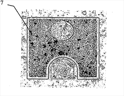
[0013] Implementations may include one or more of the following. A ball 7 rests on an interface between an ITO layer and a p-GaN layer of the LED. The balls 7 create an effective rough surface on GaN to extract more light from interior. In one implementation, the ball 7 is a sub-micron sphere with a radius of approximately 10 nm ~2um. The ball dimension is selected to optimally scatter light at approximately l/2[lambda]. In another implementation, the refractive index of the ball 7 is approximately 2.4. Suitable materials for the ball include: TiO2, Ta2O5, ZrO5 ZnO, HfO2, GaN, AlN, ZnSe5 and SiOxNy, for example. Various coating methods can be used to spread spheres on the GaN surface 42. Using an organic solution one controls the applied ball density. The sphere density can be controlled and optimized for the trade-offbetween the brightness and the electrical properties. The balls 7 are secured or held in place by applying a coating 9. The coating 9 could be conformally deposited or non-conformally deposited using various techniques such as CVD3PVD, e-beam evaporation, spin on or spray. The coating 9 should be greater than 80% transparent to the wavelength of the LED and an exemplary coating 9 can be ITO or Ni/ Au, among others
[0014] The LEDs can provide more light for the same chip size/power consumption. Alternatively, the LEDs can be made smaller given the same light output requirement and such smaller size consumes less power as well as real estate, resulting in savings. The LEDs can be fabricated with standard processing techniques making them highly cost competitive with standard LEDs.
Claims
1. A method of fabricating a semiconductor vertical light emitting diode (VLED) device, comprising: forming a multi-layer epitaxial structure of the VLED device that includes an n-gallium nitride (n-GaN) layer, an active layer, and an p-gallium nitride (p- GaN) layer; and providing a plurality of balls on a surface of the n-GaN layer of the VLED device.
2. The method as defined in Claim 1, further comprising using one of spin coating and spraying the balls on the n-GaN layer of the VLED device.
3. The method as defined in Claim 1, further comprising controlling the density of the balls by adjusting a viscosity of an applied ball-containing solution.
4. The method as defined in Claim 3, wherein the viscosity is adjusted by varying the amount and the density of balls in the applied ball-containing solution.
5. The method as defined in Claim 3, wherein the applied ball-containing solution contains one or more of: an alcohol component, a surfactant and an adhesion material.
6. The method as defined in Claim 1, further comprising securing the balls on the surface of the GaN layer of the VLED device.
7. The method as defined in Claim 2, further comprising applying a semi-transparent coating over the balls.
8. The method as defined in Claim 1, further comprising forming an electrically conductive semi-transparent coating above the balls 9. The method as defined in Claim 1, wherein the balls are planar with the n-GaN layer of the VLED device.
10. The method as defined in Claim 8, wherein the coating is greater than 80 percent transparent to the wavelength that the VLED transmits.
11. The method as defined in Claim 6, wherein the securing the balls comprises applying a transparent coat to hold the balls.
12. The method as defined in Claim 6, wherein the securing the balls comprises applying a conductive coat to hold the balls.
13. The method as defined in Claim 6, wherein the securing the balls comprises applying sol-gel to hold the balls. 14. The method as defined in Claim 6, wherein the securing the balls comprises spray coating or spin coating the balls.
15. The method as defined in Claim 1, wherein the balls are dispersed in an organic solution.
16. The method as defined in Claim 6, wherein the securing the balls comprises applying dry powder coating.
17. The method as defined in Claim 16, further comprising applying electrostatic coating to hold the balls.
18. The method as defined in Claim 8, wherein the coating comprises one of: ITO, Nickel, Gold. 19. The method as defined in Claim 1, further comprising roughening the surface of the n-GaN layer of the VLED device to scatter and extract light from interior for emission out of the n-GaN layer.
20. The method as defined in Claim 1, wherein the ball comprises a sub-micron sphere.
21. The method as defined in Claim 1, wherein the ball has a radius between approximately 10 nm and about 2micron.
22. The method as defined in Claim 1, wherein the ball dimension is selected to optimally scatter light at approximately l/2[lambda].
23. The method as defined in Claim 1, wherein a refractive index of the ball is between approximately 2.0 and 3.0. 24. The method as defined in Claim 1, wherein a refractive index of the ball is greater than approximately 2.3.
25. The method as defined in Claim 1, wherein a refractive index of the ball is approximatly equal to a refractive index of the n-GaN layer.
26. The method as defined in Claim 1, wherein the ball comprises one of: TiO2, Ta2O5, ZrO, ZnO, HfO2, GaN, AlN, ZnSe, and SiOxNy.
27. The method as defined in Claim 1, wherein the balls are spread on a surface of the n- GaN layer of the VLED device using a coating method.
28. The method as defined in Claim 1, wherein said forming of the multi-layer epitaxial structure of the VLED device is such that the emission of light by the VLED is through the n-GaN layer.
29. The method as defined in Claim 6, wherein the secured balls form a mask for dry etching the n-GaN layer.
30. The method as defined in Claim 29, wherein the etched n-GaN layer of the VLED device increases VLED surface roughness to extract more light from an interior thereof.
31. The method as defined in Claim 1, wherein the active layer is a MQW active layer.
32. The method as defined in Claim 1, further comprising depositing, over the balls, an ITO layer using one of PVD, CVD and e-beam evaporation.
33. The method as defined in Claim 1, further comprising depositing, over the balls, a transparent coating using one of: PVD, CVD and e-beam evaporation.
34. A method comprising: forming a vertical light emitting diode (VLED) device having an active layer between an n-doped layer and a p-doped layer; and securing a plurality of balls on a surface of the n-doped layer of the VLED device.
35. The method as defined in Claim 34, wherein the securing a plurality of the balls on a surface of the n-doped layer of the VLED device comprises a step selected from the group consisting of: spinning a coating over the balls; spraying a coating over the balls; applying a transparent coating over the balls; applying a semi-transparent coating over the balls; forming an electrically conductive semi-transparent coating above the balls; applying a coating over the balls that is greater than 80 percent transparent to the wavelength that the VLED transmits ; applying a conductive coat over the balls; applying sol-gel over the balls; applying a dry powder coating over the balls; applying an electrostatic coating over the balls; applying a coating over the balls comprising one of ITO, Nickel, and Gold; and applying a transparent coating using one of PVD, CVD and e-beam evaporation.
36. The method as defined in Claim 34, further comprising, prior to said securing, roughening a surface on the n-doped layer of the VLED device.
37. The method as defined in Claim 36, wherein the roughing comprises drying etching the n-doped layer using the secured balls as a mask.
38. The method as defined in Claim 34, wherein each said ball comprises a sub-micron sphere having a refractive index approximately equal to that of the n-doped layer.
39. The method as defined in Claim 34, wherein the ball comprises one of: TiO2, Ta2O5, ZrO, ZnO, HfO2, GaN, AlN, ZnSe, and SiOxNy. 40. The method as defined in Claim 34, wherein: the active layer comprises a MQW active layer; the n-doped layer comprises an n-GaN layer for emitting light from the VLED; and the p-doped layer comprises a p-GaN layer. 41. The method as defined in Claim 34, further comprising: forming an electrode in electrical communication with the n-doped layer; and forming an electrode in electrical communication with the p-doped layer.
42. A method comprising: forming, for a vertical light emitting diode (VLED) device, a MQW active layer between an n-GaN layer and a p-GaN layer; securing a plurality of balls to the n-GaN layer; and forming opposing electrodes in electrical communication, respectively, with the n-GaN layer and the p-GaN layer.
43. The method as defined in Claim 41, wherein the n-GaN layer has a roughened surface to which the plurality of balls are secured.
44. The method as defined in Claim 41, wherein light is emitted from the VLED through the n-GaN layer having a surface thereon to which the balls are secured.
See full document in pdf.
