Side view led package having lead frame structure designed to improve resin flow
The invention relates to a side view LED package in use with an LCD backlight unit. The side view LED package comprises: an LED chip; and a strip-shaped lead frame having a toothed structure formed in a lateral edge thereof. The LED chip is mounted on a surface of the lead frame. An integral package body is made of resin, and includes a hollow front half having a cavity for housing the LED chip and a solid rear half divided from the front half by the lead frame. The toothed structure of the lead frame structure can improve resin flow in order to ensure stability even if the LED package is made extremely thin.

Background of the invention
[0002] 1. Field of the Invention
[0003] The present invention relates to a side view Light Emitting Diode (LED) package in use with an LCD backlight unit. More particularly, the invention relates to a side view LED package having a lead frame structure designed to improve resin flow in order to ensure stability even if the LED package is made extremely thin.
[0004] 2. Description of the Related Art
[0005] Side view LEDs are widely used as a light source of a backlight unit of a small-sized LCD in a mobile phone, a Personal Digital Assistant (PDA) and so on. The side view LEDs are used in a package, in which their mounting height is getting gradually reduced and it is expected that a dimension of 0.5 mm or less will be required. Furthermore, the LED package should ensure high reliability while realizing high brightness by minimizing light loss and so on.
[0006] At present, in order to reduce the thickness of the side view LED package, endeavors have been made to reduce the thickness of upper and lower wall parts around an LED window. However, reducing the wall part thickness is extremely difficult task. This task also potentially weakens wall strength thereby failing to ensure reliability.
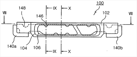
[0007] This will be described in more detail with reference to FIGS. 1 to 4, in which FIG. 1 is a front elevation view of a general side view LED package, FIG. 2 is a cross-sectional view illustrating resin flow on a plane taken along the line II-II in FIG. 1, FIG. 3 is front elevation view of a side view LED package having lead frames of the prior art, and FIG. 4 is a cross-sectional view illustrating resin flow on a plane taken along the line IV-IV in FIG. 3.
[0008] First, strip-shaped lead frames 40 are disposed in a mold as shown in FIG. 2, and resin is injected into the mold, such that resin forms a body 12 and a wall 14 surrounding a cavity C of an LED package 10 during the flow along the direction of arrow A. Resin spreads laterally in a rear half 12b of the body 12 about lead frames 40, and then directs toward a front half 12a of the body 12. In the meantime, upper and lower wall parts of the front half 12a of the body 12 are formed of resin that flows over the lead frame 40 as indicated with arrow B.
[0009] As shown in FIGS. 2 and 3, the lead frames 40 are placed along substantially the entire length of the LED package 10, with a width larger than that of the bottom 16 of the cavity C. That is, as shown in FIG. 4, the lead frames 40 are spaced from the outside surface of the body 12 at a small gap 20, which acts as a bottleneck. Therefore, it is apparent that resin does not smoothly flow along the direction of arrow B.
[0010] Then, resin insufficiently feeds to central leading ends of the upper and lower wall parts 18, thereby creating molding defects such as V-shaped voids.
[0011] In particular, since the LED package is getting longer in reverse proportion to its thickness reduction, the central leading ends of the wall parts 18 become more susceptible to molding defects.
[0012] In the meantime, heat generated from the operation of the LED chip 30 expands the lead frames 40 inside the LED package 10 along the length of the package 10. However, the lead frames 40 having different expansion coefficient from the package body 12 and an encapsulant inside the cavity C causes stress to the whole LED package 10 including the lead frames 40.
[0013] Such stress if repeated or continued may cause the lead frames 40 to get loose or separated from the package body 12 to such an extent that a disconnection A takes place between a wire W and a lead frame 40 or between the wire W and an LED chip 30 as shown in FIG. 5.
[0014] These problems are getting more serious according to the reduced thickness of the LED package 10 accompanied with its increased length.
Brief summary of the invention
[0015] The present invention has been made to solve the foregoing problems of the prior art and it is therefore an object of the present invention to provide a side view LED package having a lead frame structure designed to improve resin flow in order to ensure stability even if the LED package is made extremely thin.
[0016] It is another object of the invention to provide a side view LED package having a lead frame structure designed to ensure stability for internal electrical connection under high temperature-induced stress.
[0017] According to an aspect of the invention for realizing the object, there is provided a side view LED package comprising: an LED chip; a strip-shaped lead frame having a toothed structure formed in a lateral edge thereof, the LED chip mounted on a surface of the lead frame; and an integral package body made of resin, and including a hollow front half having a cavity for housing the LED chip and a solid rear half divided from the front half by the lead frame.
[0018] Preferably, the toothed structure of the lead frame forms a resin flow passage promoting resin to flow from the rear half to the front half of the package body. In this case, the resin flow passage may be configured to promote resin flow along a wall of the cavity from both lateral edges of thelead frame to the front half of the package body. [0019] Preferably, the toothed structure of the lead frame may comprise a groove formed in the lateral edge of the lead frame to expose a bottom of the cavity.
[0020] In this case, the groove in the lateral edge of the lead frame may be formed to such an extent that the bottom of the cavity does not directly contact the LED chip. Also, the groove in the lateral edge of the lead frame may be formed along a major part of the lead frame edge in the cavity to such an extent that a portion of the lead frame edge inserted into a wall of the cavity stably supports the lead frame. Then, a remaining part of the lead frame in the cavity may have a width of at least 80% of the thickness of the lead frame.
[0021] Preferably, the toothed structure of the lead frame as described above may further comprise a groove or hole that is fully buried in the package body.
[0022] Furthermore, the toothed structure of the lead frame may be preferably formed by punching.
[0023] Preferably, the toothed structure of the lead frame may comprise a groove or hole that is fully buried in the package body. In this case, the toothed structure of the lead frame may comprise a groove caved into the lateral edge of the lead frame from an inside wall of the cavity.
Claims
1. A side view Light Emitting Diode (LED) package comprising: an LED chip; a strip-shaped lead frame having a toothed structure formed in a lateral edge thereof, the LED chip mounted on a surface of the lead frame; and an integral package body made of resin, and including a hollow front half having a cavity for housing the LED chip and a rear half bounding on the front half by the lead frame.
2. The side view LED according to claim 1, the toothed structure of the lead frame forms a resin flow passage promoting resin to flow from the rear half to the front half of the package body.
3. The side view LED according to claim 2, wherein the resin flow passage is configured to promote resin flow along a wall of the cavity from both lateral edges of the lead frame to the front half of the package body.
4. The side view LED according to claim 1, wherein the toothed structure of the lead frame comprises a groove formed in the lateral edge of the lead frame to expose a bottom of the cavity.
5. The side view LED according to claim 4, wherein the groove in the lateral edge of the lead frame is formed to such an extent that the bottom of the cavity does not directly contact the LED chip.
6. The side view LED according to claim 4, wherein the groove in the lateral edge of the lead frame is formed along a major part of the lead frame edge in the cavity to such an extent that a portion of the lead frame edge inserted into a wall of the cavity stably supports the lead frame.
7. The side view LED according to claim 6, wherein a remaining part of the lead frame in the cavity has a width of at least 80% of the thickness of the lead frame.
8. The side view LED according to claim 2, wherein the toothed structure of the lead frame further comprises a groove or hole that is buried in the package body.
9. The side view LED according to claim 2, wherein the toothed structure of the lead frame is formed by punching.
10. The side view LED according to claim 1, wherein the toothed structure of the lead frame comprises a groove or hole that is buried in the package body.
11. The side view LED according to claim 10, wherein the toothed structure of the lead frame comprises a groove caved into the lateral edge of the lead frame from an inside wall of the cavity.
See full document in pdf.
