Electrical Considerations of LED Bulbs
Governments all over the world regulated the future use of the inefficient incandescent lamps. For example, the member states of the European Union agreed to a phasing out of incandescent lamps by 2012. The initial European-wide ban applies the first step to “nondirectional” light bulbs. The first types of bulbs to be banned are frosted (non-clear) bulbs and clear bulbs over 100 W, which will be phased out completely by September 2009. The power limit will be moved down to lower wattages, and the efficiency levels raised by the end of 2012.

.")


The replacement of 3.5 billion incandescent lamps installed throughout Europe with more-efficient lighting technologies, such as LEDs will lead to a relevant reduction in the power consumed by lighting systems.
The efficiency values and the light quality of LED bulbs are the focal point nowadays. Nevertheless, the behavior of the LED bulb technology in respect to the electrical parameters is of interest as well. LED professional has tested seven LED bulbs from four manufactures to get an inside view and reports the surprising results in this article.
Testing Conditions
Most recently produced LED bulbs from ATG Electronics, Line Lite, Exceed and Lemnis Lighting were analyzed (see Table 1). The first test stage covered the electrical parameter measurements of the mains such as input power, input current, power factor, current and voltage distortions. In the second test stage the LED bulbs were disassembled to extract the electrical circuit diagrams, and to study the mechanical designs. All tests were performed under room temperature and the devices were powered through a 500 VA electronic power amplifier simulating stable mains conditions.
See Figure 1
Measurement Results: Power Analysis
The power factors of the measured LED Bulbs showed poor values in general, ranging from 0.32 to 0.48 (see Figure 2). The low power factor values are the reasons why only 32-48% of the apparent mains power is transmitted to the LEDs as active power (see Figure 3 - LpR magazine). Nowadays, international standards claim for power factor correction circuits only for power values above 25 W. Nevertheless the reactive power has to be transferred from the power plants to the loads, ending up in unnecessary power demands and increased transmission losses.
Load Reduction Potential of Power Plants in the European Community:
Today, 3.5 billion incandescent lamps are installed in the European Community [1]. Two billion lamps are replaced each year with an intermediate lifetime of about 1,000 hours [2]. These figures imply that in average two billion lamps must be switched on for three hours every day. Due to the European time zones, it is possible that these lamps can be switched on at the same time. With an average lamp power level of 40 W (400 lm/bulb), a peak power demand calculation shows a result of 80 GW. The overall energy consumption per year can be calculated by multiplying 40 W by the intermediate lifetime by the number of replaced lamps per year, 40x1,000x2,000,000,000 = 80 TWh/a.
The replacement of the installed incandescent lamps with 8 W LED bulbs (50 lm/W, warm-white) and similar lumens output values as the incandescent lamps, would cut down the energy consumption per year to 16 TWh/a. In other words, an energy saving of 64 TWh/a could be reached, an amount that needs over 50 large 1,200 MW light water reactors. But what does this mean for the peak power load of the power plants?
The measurements showed that most of the recent LED bulbs have a relatively poor power factor resulting in a high apparent power. Hence an apparent power of 20 VA has to be calculated, in the worst case even 25 VA. As a result the peak power load is between 40 GW and 50 GW. This means a reduction between 40 - 50%, setting free a capacity of up to 25 of the named light-water reactors for other tasks. At first glance, that does not look so bad, but this is just 50% of what one would expect regarding the energy saving calculations. The reason is that only 35% of the apparent power is active power.
A replacement by LED bulbs with high-power factor values between 0.9 and 1.0 would reduce the peak power demand by an additional 50 -65%, to 16-18 GW, hence set free peak power capacity of up to 64 GW compared to incandescent lamps. Improving the power factor to 0.9-1.0 finally is the key factor to freeing up the capacities at existing power plants. It has to be recognized that most compact fluorescent lamps suffer from the same problem - at least as much as LED bulbs do. On the other hand, it has to be mentioned that there are also products available that offer power factor values of 0.85 or even more.
See Table 2 (see LpR magazine)
Measurement Results: Mains Current Distortions
The effects of the poor power factors can also be obtained at the mains input currents. Figure 4 and Figure 5 show very typical signals of the mains input currents for LED bulbs without power factor correction means. Near the input mains voltage maximum high input currents flow to charge up the internal capacitors of the LED bulbs and to supply the LEDs. The phase angle of the current flow is small and reaches only values of 10-15o. In an electrical installation, the high currents will occur at nearly the same time and will lead to a distortion of the mains voltage, generating additional wire losses. The di/dt current values of such LED bulbs vary in a wide range between 1.0 mA/μs to 253 mA/μs.
See Table 3 (see LpR magazine)
See Figure 4 (see LpR magazine)
See Figure 5 (see LpR magazine)
Figure 6 shows the mains current signal of a tested product. The phase angle of the mains current is much higher due to the usage of a passive valley fill circuitry. The switching frequency (some kHz) of the internal circuit can be measured almost unfiltered at the LED bulb mains terminals.
See Figure 6 (see LpR magazine)
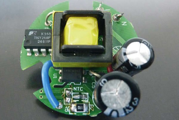
Circuit Diagrams
Typical circuit diagrams of LED bulbs are shown in Figure 7 and Figure 8. The circuit in Figure 7 uses a passive valley fill circuit in the mains input part built up with the components C1, C2, and D1-D3. This topology connects the C1 and C2 capacitor in series for the charging phase while the capacitors C1 and C2 are connected in parallel through the diodes D1 and D3 during the discharging phase. This enlarges the phase angle of the mains current flow and improves the power factor. This circuit corresponds to the signals showing in Figure 6. The high-frequency switching of the LEDs through the MOSFET Q1 leads to a high distortion of the input current and voltage. The LED strings are connected in parallel to C3. There is no galvanic isolation of the LED strings from the mains input voltage. The actual product uses only the coating material of the metal core substrate to isolate the outer parts(metal housing) from the mains voltage.
See Figure 7 (see LpR magazine)
See Figure 8 (see LpR magazine)
Figure 8 shows an improved circuit with a galvanic isolation between LED output and mains input circuit parts. Since there is no power factor correction means, the power factor is still poor and the phase angle of the current flow is low. An optocoupler (OC1) is used to close the feedback loop to guarantee the galvanic isolation.
Conclusions
Incandescent lamps are banned. The market is ready for new technologies such as LEDs. LED professional has tested seven actual LED bulb products regarding the mains parameters and the electrical circuitries to check the quality of their electrical designs.
Firstly, the security issue seems to be most important. One product uses the metal core substrate coating material to isolate the housing from the mains. Regardless of the coating specification, this seems to be insecure, e.g. in the case of a material defect or a production failure. Users are unable to recognize this security risk. Secondly, the tested products show poor power factor values. Although they are in-line with the regulations, the expectation that power plant capacities could be set free for other tasks will not be fulfilled. Thirdly, high-frequency distortions below 10 kHz could be obtained. Standard EMI tests ignore this frequency range, but in practice unwanted behaviors of installed electronic systems could occur. Lastly, the LED itself does not define the lifetime of the products. LED bulbs, e.g. with optocouplers, could get strong lifetime degradations especially at higher operating temperatures [3], which were observed in all the products.
The market entrance for new technologies such as LED bulbs is always critical, because the consumers needs confidence in these new products. This confidence can be built up with high quality and secure products where all manufacturers will gain from it. Galvanic isolated outputs, power factor values close to 1, no high-frequency disturbances at the LED bulb terminals, and a careful selection of lifetime critical components such as optocouplers are quality aspects for the design of LED bulbs. Such products will win the market race in the long run. The cost issues are important as well, but more so the potentials for further innovations.
Optocouplers – A Critical Design Element in LED Bulbs
Security issues are very important for the LED bulb electrical design. Since input to output isolation is the preferable solution, e.g. Flyback converters are an appropriate choice. One drawback of an isolated design is the feedback loop that needs to be electrically isolated too, which leads to extra efforts in the form of additional components, usually an optocoupler.
There are lots of manufacturers and products on the market and it is a challenge to make the right choice and a proper design. The products differ in price and quality in a broad range. What are the most important criteria to watch out for?
Datasheets show numerous graphs. Most of these graphs are important for a proper adjustment of the operating point and range. That may be sufficient for controlled ambient conditions. But for LED bulbs it cannot be assumed that they are operated in a narrow temperature range. On the contrary, it has to be taken into account that the bulbs can be mounted in different orientations and enclosures as well as under different ambient temperatures, which causes great variations of the working conditions. The relative current over the ambient temperature has a strong nonlinear behaviour and leads to very different light output. Another temperature dependent parameter is the collector dark currents. Even if the dark currents of modern optocouplers are very low – between some pA and some μA - they are not negligible. Such problems have to be taken into account very carefully when designing a feedback loop circuit for an LED bulb. But there are even greater issues.
LEDs are predestined for a long lifetime and most products are rated for 35,000 up to 50,000 hours. The degradation over lifetime of all components has to be matched with these lifetime expectations for the LEDs. Since optocouplers are also based on LED technology, one could argue that both LEDs will degrade almost in parallel and that could lead to compensating effects like constant light output due to an increased driver current. That may work, but the thermal stress would increase and could affect the lifetime dramatically. It also does not necessarily mean that optocoupler LEDs have the same lifetime as high quality LEDs.
Basically an optocoupler consists of an LED, a photodiode or phototransistor, and a transparent isolation in-between. Each of these components can be made of different quality and show a different aging behaviour. This behaviour is strongly dependent on the load current of the LED, the junction temperature (or component temperature), and the material and manufacturing dependent parameters.
In a “General Description” document [1] from Vishay Semiconductors, it is shown that the current transfer ratio of a high quality product degrades by 5% over 100,000 hours at 60 mA and a junction temperature of 60° C, but by 30% at a junction temperature of 125° C. Such degradation could be caused by each component of the optocoupler; the LED or the photodetector, or loss of transparency of the isolating resin, or the sum of all these factors.
In a study on the “Reliability of Optoelectronic Elements” from Ivan Stanchev Kolev and Tsanko Vladimirov Karadzhov [2] failure frequency in dependency of the previously mentioned factors was researched and different design instructions were proposed:
• Operation of LEDs at low temperature, if necessary cooling of LEDs
• Operation with a low LED current and a low mark-to-space ratio
• Usage of optocouplers with a high CTR (Ki)
• High resistive output load
• Usage of negative optical feedback
• Operation with the LED current below 50% of the datasheet value
• Usage of heteroLEDs
In addition, the authors proposed compensation circuits for the LED, the phototransistor circuit or both (Figure 1).
See Figure 9 (see LpR magazine)
J.Ben Hadj Slama et al. [3] point out that after an accelerated thermal aging with a Tj of 105° C photodetector aging was negligible, whereas LED degradation, especially for lower currents, was significant. All other performed tests indicate also that LED degradation is the most important issue. It was also shown, that higher currents have more influence than higher ambient temperatures if Tj is identical for both situations. Based on these results the team developed a model that fits quite well for a degradation prediction above 200 hours.
Agilent offers information on aging and reliability of optocouplers in a designer guideline [4]. The aging was performed at an ambient temperature of 125° C with 25 mA and 100% duty cycle. To extend lifetime Agilent recommends lowering IF clearly below the stress current of 25 mA, e.g. down to 5 mA. In addition duty cycles below 100% will help to reduce degradation as well as lowering ambient temperatures. All these provisions result in a lower junction temperature, which is seen to be the main reason for degradation. AlGaAs LEDs show lower degradation over time than GaAsP LEDs based optocouplers and, hence are the better choice.
Motorola also analyzed lifetime behaviour of optocouplers with very similar results to Agilent [5]. At a moderate ambient temperature of 40°C the absolute difference between IF of 1 mA and 50 mA was relatively small with a degradation of a few percent after 50,000 hours. At an ambient temperature of 70°C for both currents, degradation was much higher, but degradation for IF = 1 mA was still acceptable with 6% after 50,000 hours. Nevertheless, for batch variations that would be typically seen in a large volume production they propose a 6-sigma correction, which leads to a degradation limit of 25% instead of 6%.
All studies show strong dependencies of degradation from ambient temperature and the LED forward current IF. The forward current can be controlled by the design where the ambient temperature is a given parameter. In LED bulb applications the optocouplers are integrated within the heat sinks which can reach temperatures of 60-70°C at an ambient temperature of 25°C, and the optocouplers are exposed to ambient temperatures of 70°C. Compensation circuits as proposed from Ivan Stanchev Kolev, et al. could help to prevent damage. As an alternative to optocouplers, the auxiliary windings of the Flyback transformers could be used for feedback issues, or new driver ICs could allow for designs with primary side feedback systems.
