Light emitting diodes packaged for high temperature operation
In accordance with the invention, an LED packaged for high temperature operation comprises a metal base including an underlying thermal connection pad and a pair of electrical connection pads, an overlying ceramic layer, and a LED die mounted overlying the metal base. The LED is thermally coupled through the metal base to the thermal connection pad, and the electrodes are electrically connected to the underlying electrical connection pads. A low thermal resistance insulating layer can electrically insulate other areas of die from the base while permitting heat passage. Heat flow can be enhanced by thermal vias to the thermal connector pad. Ceramic layers formed overlying the base can add circuitry and assist in distributing emitted light. The novel package can operate at temperatures as high as 250.degree. C.


Background of the invention
Light emitting diodes (LEDs) are being used as light sources in an increasing variety of applications extending from communications and instrumentation to household, automotive and visual display. Many of these applications require higher levels of power or subject the LEDs to higher temperature operating environments. In response, LED manufacturers have improved the purity of the semiconductor materials in order to keep the LED output intensity high as temperature increases. As a result, desired applications of LEDs are now constrained by the thermal limits of their packaging.
The currently prevalent plastic LED packages have an operational temperature limit of about 80.degree. C. Some LED die, however, will operate at 120.degree. C., and industry preference is for an operational temperature of about 200.degree. C. Accordingly there is a need for an improved light emitting diode packaged for high temperature operation.
Brief summary of the invention
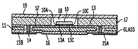
In accordance with the invention, an LED packaged for high temperature operation comprises a metal base including an underlying thermal connection pad and a pair of electrical connection pads, an overlying ceramic layer, and a LED die mounted overlying the metal base. The LED is thermally coupled through the metal base to the thermal connection pad, and the electrodes are electrically connected to the underlying electrical connection pads. A low thermal resistance insulating layer can electrically insulate other areas of die from the base while permitting heat passage. Heat flow can be enhanced by thermal vias to the thermal connector pad. Ceramic layers formed overlying the base can add circuitry and assist in distributing emitted light. The packaged diode can be made by the low temperature co-fired ceramic on metal technique (LTCC-M). The LTCC-M packaged diode can operate at temperatures as high as 250.degree. C.
Claims
1. A low temperature co-fired ceramic on metal (LTCC-M) light emitting diode (LED) assembly for high temperature operation comprising: a metal base, the metal base including a thermal connection surface; at least one LED die, the LED die having a pair of electrodes overlying and electrically insulated from the metal base by an insulating layer, the die thermally coupled through the metal base to the thermal connection surface; a layer of ceramic overlying the metal base, the layer of ceramic having at least one opening to house the LED die; a plurality of conductive traces insulated from the metal base, the LED electrodes electrically connected to the conductive traces; and one or more isolated terminals formed on the metal base, the one or more isolated terminals electrically connected to decoder/driver electronics that control the LED electrodes, wherein the electronics are mounted within the assembly.
2. The LED assembly of claim 1 further comprising a plurality of edge connector fingers, wherein the fingers are connected to the LED electrodes.
3. The LED assembly of claim 1 further comprising an additional metal block on which the LED assembly is mounted to further improve heat dissipation.
4. The LED assembly of claim 1 wherein the LED die is a flip-chip.
5. The LED assembly of claim 4 wherein the flip-chip is bonded to the traces by conductive balls comprising solder or gold.
6. The LED assembly of claim 1 further comprising vias in the insulating layer, the vias electrically connecting the traces to the isolated terminals.
7. A low temperature co-fired ceramic on metal (LTCC-M) light emitting diode (LED) assembly for high temperature operation comprising: a metal base, the metal base including a thermal connection surface; at least one LED die, the LED die having a pair of electrodes overlying and electrically insulated from the metal base by an insulating layer, the die thermally coupled through the metal base to the thermal connection surface; a layer of ceramic overlying the metal base, the layer of ceramic having at least one opening to house the LED die; a plurality of conductive traces insulated from the metal base, the LED electrodes electrically connected to the conductive traces; and a plurality of edge connector fingers, wherein the fingers are connected to decoder/driver electronics embedded in the assembly that control the LED electrodes.
8. The LED assembly of claim 7 further comprising an additional metal block on which the LED assembly is mounted.
9. The LED assembly of claim 7, wherein the LED die is a flip-chip.
10. The LED assembly of claim 9, wherein the flip-chip is bonded to the traces by one or more conductive balls.
11. A light emitting diode (LED) assembly for high temperature operation comprising: a metal base, the metal base including a thermal connection surface; at least one LED die, the LED die having a pair of electrodes overlying and electrically insulated from the metal base by an insulating layer, the die thermally coupled through the metal base to the thermal connection surface; a layer of electrically insulating material overlying the metal base, wherein the layer of electrically insulating material includes at least one opening to house the LED die; a plurality of conductive traces insulated from the metal base, the LED electrodes electrically connected to the conductive traces; and one or more isolated terminals formed on the metal base, the one or more isolated terminals electrically connected to decoder/driver electronics that control the LED electrodes, wherein the electronics are mounted within the assembly.
12. The LED assembly of claim 11 further comprising a plurality of edge connector fingers, wherein the fingers are connected to the LED electrodes.
13. The LED assembly of claim 11 further comprising an additional metal block on which the LED assembly is mounted to further improve heat dissipation.
14. The LED assembly of claim 11 wherein the LED die is a flip-chip.
15. The LED assembly of claim 13 wherein the flip-chip is bonded to the traces by conductive balls comprising solder or gold.
16. The LED assembly of claim 11 further comprising vias in the insulating layer, the vias electrically connecting the traces to the isolated terminals.
17. A light emitting diode (LED) assembly for high temperature operation comprising: a metal base, the metal base including a thermal connection surface; at least one LED die, the LED die having a pair of electrodes overlying and electrically insulated from the metal base by an insulating layer, the die thermally coupled through the metal base to the thermal connection surface; a layer of electrically insulating material overlying the metal base, the layer of electrically insulating material having at least one opening to house the LED die; a plurality of conductive traces insulated from the metal base, the LED electrodes electrically connected to the conductive traces; and a plurality of edge connector fingers, wherein the fingers are connected to decoder/driver electronics embedded in the assembly that control the LED electrodes.
18. The LED assembly of claim 17 further comprising an additional metal block on which the LED assembly is mounted.
19. The LED assembly of claim 17, wherein the LED die is a flip-chip.
20. The LED assembly of claim 19, wherein the flip-chip is bonded to the traces by one or more conductive balls.
See full document in pdf.
