Thin gallium nitride light emitting diode device
Disclosed is a light emitting diode (LED) device that comprises a crystal structure of a sapphire substrate-free gallium nitride (GaN) LED, wherein the crystal structure is mounted on a first surface of a sub-mount substrate in the form of a unit chip, and the first surface of the sub-mount substrate has a surface area greater than the surface area of a region in which the unit chip is bonded. Preforms for manufacturing the LED device and a method for manufacturing the LED device are also disclosed. The sapphire substrate, on which the crystal structure of the light emitting diode has grown, is processed into a unit chip before being removed. Thus, any crack in the crystal structure of the light emitting diode that may occur during the removal of the sapphire substrate can be prevented. Therefore, a thin light emitting diode device can be manufactured in a mass production system.

Background of the invention
[0004] In general, a light emitting diode (LED) device is a semiconductor device that generates light by causing electric current to flow through a PN junction in the forward direction.
[0005] LEDs using a semiconductor have been the focus of attention in the field of applied lighting equipments of next generation, due to their advantages of having high efficiency in converting electric energy to light energy, a long lifespan of more than 5 to 10 years, and high cost efficiency resulting from reduced maintenance cost and low power consumption.
[0006] Sapphire substrates are widely used to grow the GaN-based compound semiconductors for use in the manufacture of LEDs. Sapphire substrates are electric insulators, constructed so that the anodes and cathodes of LEDs are formed on the front surface of a wafer.
[0007] In general, a top emission type GaN light emitting diode is widely used in low-output applications. As shown in FIG. 1a, a GaN LED is manufactured by a process comprising the steps of: placing a sapphire substrate 10, on which a crystal structure has grown, on a lead frame 20, and then connecting two electrodes 11 and 12 with the top portion of the sapphire substrate 10. At this time, in order to improve the heat dissipation rate, the sapphire substrate is bonded to the lead frame after reducing its thickness to about 100 micron or less.
[0008] However, thermal conductivity of a sapphire substrate is about 50 W/mK. Therefore, even if the thickness is reduced to about 100 micron, it is difficult to obtain the desired heat dissipation property with the arrangement as shown in FIG. 1a, due to the significantly high thermal resistance.
[0009] Thus, it is the current trend to employ a flip-chip bonding technique as shown in FIG. 1b to further improve the heat dissipation property of a high output GaN light emitting diode. In the flip-chip bonding technique, a chip with an LED structure, which has grown on the sapphire substrate, is flip over upside down, and is bonded to a sub-mount substrate 30, such as a silicon wafer or an AlN ceramic substrate having excellent thermal conductivity (about 150 W/mK or 180 W/mK). In this case, because the heat dissipation is made through the sub-mount substrate, the heat dissipation rateis improved compared to the heat dissipation made through the sapphire substrate. However, the improvement is not so satisfactory.
[0010] With regard to the above-mentioned problem, a thin film type GaN LED without a sapphire substrate has been suggested recently. A typical method for manufacturing an LED by removing the sapphire substrate comprises removing the sapphire substrate from the crystal structure of the LED by way of laser lift-off technique before packaging. This method is known to provide the highest heat dissipation rate.
[0011] Furthermore, unlike the flip-chip bonding technique, such removal of the sapphire substrate by way of lift-off technique does not require a delicate flip-chip bonding process, and is comprised of simple processing steps if the problem related with the removal of the sapphire substrate is solved. Also, the sapphire substrate-free thin film type LED shows superior properties to the LED manufactured by the flip-chip bonding technique, because the former LED has a light emitting area of about 90% of the size of chips, while the latter LED has a light emitting area of about 60% of the size of chips.
[0012] Despite the aforementioned advantages, however, the conventional laser lift-off technique widely used for removing sapphire substrates is not yet applicable to mass production. This is because the conventional laser lift-off technique causes structural crack in the LED crystal due to the stress present between the sapphire substrate and the crystal structure of the LED upon the irradiation of laser, and thus provides significantly low yield in spite of excellent heat dissipation property.
[0013] Therefore, there is an imminent need for a method for manufacturing a sapphire substrate-free thin film type GaN light emitting diode, having excellent light emission efficiency and heat dissipation efficiency, in mass quantity.
Brief summary of the invention
The present invention relates to a novel thin light emitting diode device, which has improved light emitting efficiency and heat dissipation rate, and preforms and a method for manufacturing the same.
Claims
1. A light emitting diode (LED) device that comprises a crystal structure of a sapphire substrate-free gallium nitride (GaN) LED, wherein the crystal structure is mounted on a first surface of a sub-mount substrate in the form of a unit LED chip, and the first surface of the sub-mount substrate has a surface area greater than the surface area of a region in which the unit chip is bonded.
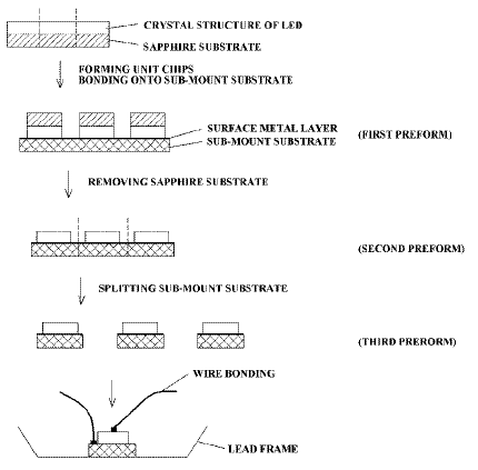
2. The light emitting diode device according to claim 1, which is obtained by the steps of: a first step of splitting the sapphire substrate, on which the crystal structure of the GaN LED has grown, into unit LED chips; a second step of bonding at least one unit chip to the sub-mount substrate; and a third step of removing the sapphire substrate from the unit chip.
3. The light emitting diode device according to claim 2, which is obtained by bonding at least two unit chips, spaced apart from each other, to the sub-mount substrate in the second step, and cutting the sub-mount substrate between two adjacent unit chips after the third step, so that each sub-mount substrate has at least one unit chip.
4. The light emitting diode device according to claim 2, which is obtained by bonding a single unit chip to the sub-mount substrate in the second step, wherein the first surface of the sub-mount substrate has an area greater than the surface area of the region in which the unit chip is bonded.
5. The light emitting diode device according to claim 1, wherein the unit LED chip has a size of 0.2.times.0.2.about.5.times.5 mm.sup.2.
6. The light emitting diode device according to claim 2, wherein the sub-mount substrate is a wafer with a diameter of 1.about.6 inches. 7. The light emitting diode device according to claim 1, wherein the sub-mount substrate having the unit chip is mounted on a lead frame. 8. The light emitting diode device according to claim 1, wherein a metal layer is formed on the first surface of the sub-mount substrate, and the metal layer is exposed on the surface of the sub-mount substrate extending from a circumference of the region in which the unit chip is bonded.
9. The light emitting diode device according to claim 8, wherein the exposed metal layer serves as a reflection layer with a high light reflection ratio.
10. The light emitting diode device according to claim 8, wherein the exposed metal layer is subjected to wire bonding.
11. The light emitting diode device according to claim 8, wherein the metal layer is formed of at least one metal selected from the group consisting of Pt, Rh, Ru and Au, or alloys thereof.
12. The light emitting diode device according to claim 1, wherein the sub-mount substrate is comprised of a conductive material, and is connected directly to a p-ohmic contact electrode and a metal pad for heat sink area of a lead frame.
13. The light emitting diode device according to claim 2, wherein the sapphire substrate, on which the crystal structure of the light emitting diode has grown, is subjected to dry etching in a portion to be present as edges of the unit chip, before splitting the sapphire substrate, so as to provide flat lateral surfaces to the crystal structure of the light emitting diode present in the unit chip.
14. The light emitting diode device according to claim 2, wherein surface roughening is formed on the surface of the crystal structure of the LED, exposed upon the removal of the sapphire substrate, by way of dry or wet etching treatment.
15. The light emitting diode device according to claim 2, wherein a molding portion is formed on the GaN semiconductor layer on the surface of the crystal structure of the light emitting diode, exposed upon the removal of the sapphire substrate, the molding portion being formed by coating the GaN semiconductor layer with a mixture containing a molding material and a material transparent to visible light, whose refractive index is substantially equal to refractive index of the GaN semiconductor layer, and then with the molding material.
16. The light emitting diode device according to claim 15, wherein the surface of the crystal structure of the light emitting diode, exposed upon the removal of the sapphire substrate, is an n-type GaN semiconductor layer, and the material transparent to visible light, whose refractive index is equal to refractive index of the n-type GaN semiconductor layer, is TiO.sub.2 powder.
17. The light emitting diode device according to claim 2, wherein the surface of the crystal structure of the light emitting diode, exposed upon the removal of the sapphire substrate, is an n-type GaN semiconductor layer, and the n-ohmic contact on the n-type GaN semiconductor layer is formed from at least one ohmic contact area for wire bonding pad or from a combination of at least one ohmic contact area for wire bonding pad with an ohmic contact strip line.
18. A first preform for manufacturing a light emitting diode device that comprises a sapphire substrate, on which a crystal structure of a GaN light emitting diode has grown, mounted on a sub-mount substrate in the form of at least two unit chips.
19. The first preform for manufacturing a light emitting diode device according to claim 18, wherein a pattern that displays a position, in which the unit chip is bonded, or a pattern that displays a position, in which the sub-mount substrate is split into the unit chip, is formed on the sub-mount substrate.
20. The first preform for manufacturing a light emitting diode device according to claim 18, wherein at least two unit chips are bonded periodically to a single sub-mount substrate, while being spaced apart at a predetermined interval between two adjacent unit chips.
21. The first preform for manufacturing a light emitting diode device according to claim 18, wherein adjacent unit chips have an interval controlled to prevent each unit chip being placed over an edge of a region to be subjected to irradiation of laser beams, when removing the sapphire substrate with laser. 22. The first preform for manufacturing a light emitting diode device according to claim 18, wherein a metal layer is formed on the first surface of the sub-mount substrate having the sapphire substrate, on which a crystal structure of a GaN light emitting diode has grown, mounted in the form of unit chips.
23. A second preform for manufacturing a light emitting diode device, which is obtained from the first preform for manufacturing a light emitting diode device according to claims 18, which comprises a sapphire substrate, on which the crystal structure of a GaN light emitting diode has grown, mounted on a sub-mount substrate in the form of at least two unit chips, by removing the sapphire substrate.
24. A third preform for manufacturing a light emitting diode device, which is obtained from the first preform for manufacturing a light emitting diode device according to claim 18, which comprises a sapphire substrate, on which the crystal structure of a GaN light emitting diode has grown, mounted on a sub-mount substrate in the form of at least two unit chips, by removing the sapphire substrate, and then by cutting the sub-mount substrate in a position between two adjacent unit chips.
25. A method for manufacturing a light emitting diode device by allowing a crystal structure of a gallium nitride light emitting diode to grow on a sapphire substrate, which comprises the steps of: splitting the sapphire substrate, on which the crystal structure of the light emitting diode has grown, into a unit chip; and removing the sapphire substrate from the unit chip.
26. The method for manufacturing a light emitting diode according to claim 25, which further comprises, before the step of removing the sapphire substrate, a step of bonding at least one unit chip to a sub-mount substrate after splitting the sapphire substrate, on which the crystal structure of the light emitting diode has grown, into a unit chip.
27. The method for manufacturing a light emitting diode according to claim 26, wherein at least two unit chips are bonded to the sub-mount substrate in the unit chip bonding step, and the method further comprises a step of cutting the sub-mount substrate in such a manner that the sub-mount substrate has at least one unit chip, after the step of removing the sapphire substrate.
28. The method for manufacturing a light emitting diode according to claim 27, wherein at least two unit chips, bonded to a single sub-mount substrate, are arranged periodically, while being spaced apart at a predetermined interval between adjacent two unit chips, when bonding at least two unit chips to the sub-mount substrate.
29. The method for manufacturing a light emitting diode according to claim 25, wherein the sapphire substrate is removed by way of laser in the step of removing the sapphire substrate.
30. The method for manufacturing a light emitting diode according to claim 26, wherein at least one unit chip is bonded to the sub-mount substrate in such a manner that adjacent unit chips have a interval controlled to prevent each unit chip being placed over an edge of a region to be subjected to irradiation of laser beams, when removing the sapphire substrate with laser.
31. The method for manufacturing a light emitting diode according to claim 29, wherein the laser has a wavelength ranging from 200 nm to 365 nm.
32. The method for manufacturing a light emitting diode according to claim 25, wherein the crystal structure of the light emitting diode is allowed to grow on the sapphire substrate having a metal buffer layer formed thereon, and the sapphire substrate is removed by dissolving the metal buffer layer in the step of removing the sapphire substrate.
33. The method for manufacturing a light emitting diode according to claim 26, wherein at least two unit chips, spaced apart from each other at a predetermined interval, are bonded to the sub-mount substrate, and the sub-mount substrate is cut in a position between two adjacent unit chips, or only one unit chip is bonded to a sub-mount substrate larger than the surface area of the region in which the unit chip is bonded, and a surface of the sub-mount substrate extending from the circumference of the region, in which the unit chip is bonded, is subjected to wire bonding. 34. The method for manufacturing a light emitting diode according to claim 26, wherein at least one unit chip is bonded to the sub-mount substrate having a metal layer formed thereon.
See full document in pdf.
