Aluminum Nitride Light Emitting Diodes with the Shortest Wavelength towards Dioxin, PCB Decomposition Technology
Nippon Telegraph and Telephone Corporation (NTT) has observed light of 210-nm wavelength from aluminum nitride (AlN) light emitting diodes (LED).
: AlN Deep-Ultraviolet Light-Emitting Diode")


: High-Purity AlN Crystal Fabrication Technology")
: p-type, n-type Doping Technologies")
: 210-nm Light Emission; World's Shortest")
This is the shortest wavelength ever observed from any semiconductor, and confirms the long-held theoretical expectation that AlN could emit light in the deep ultraviolet (DUV) region (1) (wavelengths from 200 to 300 nanometers; nano is 10-9). Light emitted at wavelengths in the DUV can efficiently decompose persistent toxic substances such as dioxin and PCBs (2) , which have caused serious environmental problems all over the world. Therefore, our AlN LED promises to have a major environmental impact. In addition, AlN semiconductor itself is harmless, unlike the mercury lamp. Replacing gas lasers with high-power AlN DUV lasers could lead to small, highly reliable, and highly efficient nanometer fabrication. The major problem in AlN LED fabrication had been high densities of crystalline defects and high impurity concentrations. NTT has overcome these problems by developing technologies for high-purity AlN crystal fabrication and for p-type and n-type doping (3) , which are essential for LED fabrication. This achievement is the first step towards practical AlN LEDs, but is a giant step in science, and will be reported in "Nature" magazine, May 18 issue.
Features
(1) Fabrication technology of high-pure AlN semiconductor.
(2) p-type and n-type doping technologies essential for LEDs.
(3) Observation of deep ultraviolet light, 210nm, the shortest in the world.
(4) AlN LEDs will replace conventional gas sources such as mercury lamp
Background
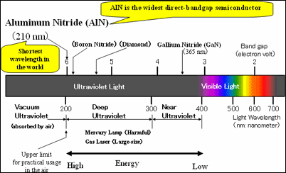
Aluminum nitride (AlN) has the widest direct band gap among semiconductors (4) , Therefore, it has always been expected theoretically that an AlN light-emitting device would emit light with the shortest wavelength among semiconductors (figure1). However, AlN has had a high density of crystalline defects and the p-type and n-type doping technologies essential for LEDs were not available. Of course, AlN LEDs have not been achieved. At present, blue and ultra-violet gallium nitride (GaN) LEDs and laser diodes are commercially available, but their shortest wavelength is 365nm, still in the near-ultraviolet region.
The deep ultraviolet (DUV) light sources available at present are only gas sources, such as mercury lamps or gas lasers. Mercury lamps and gas lasers use toxic substances, and gas lasers have practical problems: the gas has to be supplied often and the lasers are large and inefficient. Replacing these light sources with semiconductor devices will save space and greatly improve reliability and efficiency. DUV light has very short wavelength, and can be focused to spots only tens of nanometers in diameter (figure2). It therefore can be applied to nanometer-scale fabrication and to submicron-particle detection. In addition, the energy of DUV light is high enough to decompose very stable substances. Therefore, DUV LEDs are expected to have a wide range of applications, such as in environmental protection, nanotechnology, information technology, medical treatment, sanitation, and biology.
Technology
(1) High-purity AlN fabrication technology NTT noticed that the purity could be improved by reducing crystalline defects and impurities (5) . Therefore, NTT constructed AlN fabrication system that could endure fabrication temperatures as high as 1100°C and prevent secondary reactions of composite aluminum and nitrogen sources. As a result, we were able to decrease defect density and impurity concentration by one order and produce high-purity AlN crystal (figure3).
(2) AlN p-type and n-type doping technologies In this high-purity AlN, by doping magnesium (Mg) to AlN we achieved p-type AlN, and, similarly, by doping silicon (Si) to AlN, we achieved n-type AlN (figure4).
(3) AlN deep-ultraviolet (DUV) light-emitting diodes (LEDs) Next, we formed a high-purity AlN light-emitting layer sandwiched by p-type and n-type AlN layers and fabricated AlN LEDs (figure5).
When current flowed through the AlN LEDs, we observed 210-nm DUV light (figure6).
Future plan
By further decreasing crystalline defects and impurities and by improving doping technologies, NTT intends to improve the output power of AlN LEDs, which should lead to practical use.
Terminology
*1 Deep ultraviolet (DUV) light, Neat ultraviolet light
Light at wavelengths shorter than 400nm is called ultraviolet light. Ultraviolet light in the wavelength region from 200 to 300nm is called deep ultraviolet (DUV) light, and ultraviolet light in the wavelength region from 300 to 400nm is called near ultraviolet light. Ultraviolet light with a wavelength shorter than 200nm is absorbed by air, and therefore cannot be used in air. Therefore, it is called vacuum ultraviolet light. Thus, the wavelengths of DUV light are shortest at which light can be used in air. The shorter the wavelength is, the smaller the area in which light can be concentrated and the higher the energy becomes.
*2 Dioxin, PCB
Dioxin and PCB (polychlorinated biphenyls) are very toxic but very stable chemically. One way to decompose them chemically and to make them harmless is to expose them to DUV light. Conventional DUV light sources are gas sources, and therefore are not practical. But if practical AlN LEDs can be built, we will have an invaluable light source for the decomposition of harmful chemical substances.
*3 p-type, n-type doping technologies Adding a small amount of dopant to pure semiconductors can drastically change their electric properties. With p-type doping, holes, positively charged carriers, can be supplied, and with n-type doping, electrons, negatively charged carriers, can be supplied. In LEDs or semiconductor lasers, holes are supplied from a p-type layer and electrons from an n-type layer to the light-emitting layer, and when holes and electrons combine, light is emitted. Therefore, p-type and n-type doping technologies are essential for LEDs or semiconductor lasers.
*4 Direct band gap semiconductor
From its physical properties, any semiconductor has either a direct band gap or an indirect band gap. In direct band gap semiconductors, electrons and holes combine directly, and the efficiency of light emitting is therefore very high. Therefore, direct band gap semiconductor is suitable for LEDs and semiconductor lasers. In contrast, in indirect band gap semiconductors, electrons and holes combine indirectly, and efficiency of light emission is very low. Therefore, indirect band gap semiconductor is not suitable for light-emitting devices.
For example, diamond and boron nitride (BN) have wide band gap energies similar to that of AlN, but because they are indirect band gap semiconductors, they are not suitable for LEDs.
Band gap
In a semiconductor, there is forbidden energy gap between the electron-allowed and hole-allowed bands. The band gap energy is inversely proportional to the wavelength of light emitted from a semiconductor. AlN has the widest band gap energy among direct band gap semiconductors and can therefore emit the shortest light.
*5 Crystalline defect, impurity
Ideally in AlN crystal, aluminum (Al) and nitrogen (N) atoms order periodically. However, if the crystal has any anomalies, there will be vacancies at which an Al or N atom sit and these vacancies become crystalline defects. If there are atoms other than Al or N, such as oxygen, those atoms become impurities. When crystalline defects or impurities exist and p-type or n-type doping is tried, the dopants capture generated holes or electrons, and p-type or n-type semiconductor is not formed.
In the case of AlN, because Al and N atoms are attracted strongly to each other, during crystal fabrication, secondary reactions between Al and N sources can easily occur. As a result, in AlN, crystalline defects and impurities occur very easily.
{mosgoogle}
Authors Daniel L. Barton and Arthur J. Fischer Semiconductor Material and Device Sciences, Sandia National Labs. Albuquerque, NM Dr. Barton has authored and presented several contributed and invited papers at SPIE Photonics West including a chapter in an SPIE critical review book on gallium nitride-based technologies. http://www.sandia.gov/1100 Dr. Fischer is a Principal Memeber of the Technical Staff at Sandia National Laboratories. He has been leading the research at Sandia on photonic crystals for solid state lighting and other potential applications. References: 1. S. J. Smith, E. M. Purcell, Visible Light from Localized Charges Moving across a Grating, Phys. Rev, Vol: 92, no. 4, pp. 1069, 1953. 2. E. Yablanovich, Inhibited Spontaneous Emission in Solid-State Physics and Electronics, Phys. Rev. Lett., Vol: 55, no. 20, pp. 2059, 1987. 3. Jonathan J. Wierer, Michael R. Krames, John E. Epler, Nathan F. Gardner, Joel R. Wendt, Mihail M. Sigalas, Steven R. J. Brueck, Dong Li, Michael Shagam, III-nitride LEDs with photonic crystal structures, Proc. SPIE, Vol: 5739, pp. 102-107, 2005.
Future plan
By further decreasing crystalline defects and impurities and by improving doping technologies, NTT intends to improve the output power of AlN LEDs, which should lead to practical use.
Terminology
*1 Deep ultraviolet (DUV) light, Neat ultraviolet light
Light at wavelengths shorter than 400nm is called ultraviolet light. Ultraviolet light in the wavelength region from 200 to 300nm is called deep ultraviolet (DUV) light, and ultraviolet light in the wavelength region from 300 to 400nm is called near ultraviolet light. Ultraviolet light with a wavelength shorter than 200nm is absorbed by air, and therefore cannot be used in air. Therefore, it is called vacuum ultraviolet light. Thus, the wavelengths of DUV light are shortest at which light can be used in air. The shorter the wavelength is, the smaller the area in which light can be concentrated and the higher the energy becomes.
*2 Dioxin, PCB
Dioxin and PCB (polychlorinated biphenyls) are very toxic but very stable chemically. One way to decompose them chemically and to make them harmless is to expose them to DUV light. Conventional DUV light sources are gas sources, and therefore are not practical. But if practical AlN LEDs can be built, we will have an invaluable light source for the decomposition of harmful chemical substances.
*3 p-type, n-type doping technologies Adding a small amount of dopant to pure semiconductors can drastically change their electric properties. With p-type doping, holes, positively charged carriers, can be supplied, and with n-type doping, electrons, negatively charged carriers, can be supplied. In LEDs or semiconductor lasers, holes are supplied from a p-type layer and electrons from an n-type layer to the light-emitting layer, and when holes and electrons combine, light is emitted. Therefore, p-type and n-type doping technologies are essential for LEDs or semiconductor lasers.
*4 Direct band gap semiconductor
From its physical properties, any semiconductor has either a direct band gap or an indirect band gap. In direct band gap semiconductors, electrons and holes combine directly, and the efficiency of light emitting is therefore very high. Therefore, direct band gap semiconductor is suitable for LEDs and semiconductor lasers. In contrast, in indirect band gap semiconductors, electrons and holes combine indirectly, and efficiency of light emission is very low. Therefore, indirect band gap semiconductor is not suitable for light-emitting devices.
For example, diamond and boron nitride (BN) have wide band gap energies similar to that of AlN, but because they are indirect band gap semiconductors, they are not suitable for LEDs.
Band gap
In a semiconductor, there is forbidden energy gap between the electron-allowed and hole-allowed bands. The band gap energy is inversely proportional to the wavelength of light emitted from a semiconductor. AlN has the widest band gap energy among direct band gap semiconductors and can therefore emit the shortest light.
*5 Crystalline defect, impurity
Ideally in AlN crystal, aluminum (Al) and nitrogen (N) atoms order periodically. However, if the crystal has any anomalies, there will be vacancies at which an Al or N atom sit and these vacancies become crystalline defects. If there are atoms other than Al or N, such as oxygen, those atoms become impurities. When crystalline defects or impurities exist and p-type or n-type doping is tried, the dopants capture generated holes or electrons, and p-type or n-type semiconductor is not formed.
In the case of AlN, because Al and N atoms are attracted strongly to each other, during crystal fabrication, secondary reactions between Al and N sources can easily occur. As a result, in AlN, crystalline defects and impurities occur very easily.
{mosgoogle}
Authors
