Development of Gallium Nitride Wafers Nearly Doubling Green LED Luminous Efficiency
The GaN wafers developed by NGK feature low defect density across the entire 2-inch diameter of the wafer surface and have a colorless transparency. NGK achieved this through proprietary improvements to liquid phase epitaxial technology for single crystal growth.
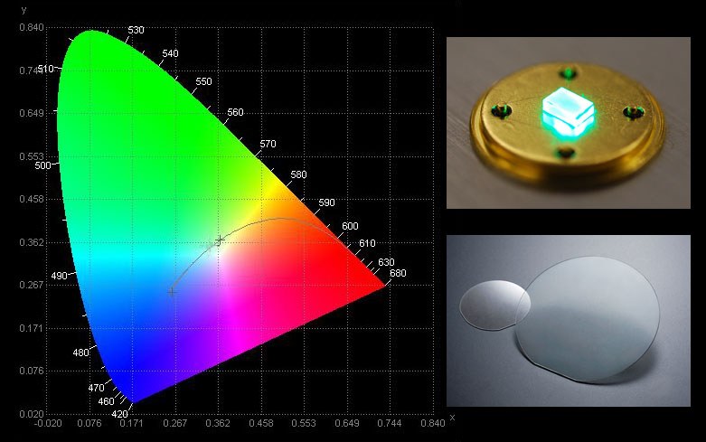

In joint research carried out with Nagoya University, green LED chips formed on the NGK GaN wafers showed a 60% internal quantum efficiency*1 (injection current density of approximately 200 amperes per square centimeter). This figure is roughly double that of the green LED chips currently on the market. The results were jointly announced at the International Workshop on Nitride Semiconductors 2012 (IWN 2012) held in Sapporo, Hokkaido (Japan) from October 14-19, 2012.
In previous LED chips using sapphire wafers as substrates, defects of light emission layer were common, especially for green LEDs. These defects prevented a large operation current, which in turn prevented the LEDs from achieving sufficient brightness. This issue can be addressed by the use of the low-defect GaN wafers produced by NGK as substrates that enable dramatically improved light emission layer quality. The reduction in current loss that results allows for a large current, making high brightness green LED elements a reality. When these elements are used to make up green LED light sources, the result is an improvement in brightness of more than 20 times*2 compared to previous models. Light sources can also be made more compact thanks to the simplified heat dissipation structure made possible by less heat generated from current loss. This control of heat-related degradation also enables longer product life.
The realization of high brightness green LED light sources means that high brightness LED light sources are now available for the primary colors of light (red, green and blue). We can thus expect to see advancements in the development of new applications for LEDs, specifically for use in projectors and other imaging applications.
This emerging potential for green LED applications follows on the heels of an announcement of applications for blue LEDs on April 25, 2012. NGK is now poised to apply its technology to the inverters used in hybrid and electric vehicles, power amplifiers for base stations of wireless communication, and other power devices. To this end, NGK will take steps to further reduce defect density for its GaN wafers, and to produce larger wafers that are greater than 6 inches in diameter.
Sample shipments of 2-inch-diameter wafers are already under way, with shipment of 4-inch samples also set to begin in 2012. Plans call for raising production capacity from the current level of 200 wafers per month (2-inch wafer) to a monthly output of over 1,000 wafers during fiscal 2012. By 2014, NGK plans to have a wide-ranging lineup of wafers extending from 2- to 6-inch-diameter wafers ready for LED and power device applications.
*1 Internal quantum efficiency: Ratio of the number of electrons (current) injected into an LED to the number of photons generated in the emission layer. The ratio is dependent on the crystal defect density in the emission layer and the ideal ratio is 100%.
*2 “More than 20 times”: For example, if LED elements with an internal quantum efficiency twice that of previous models are paired with a 10 times greater flow of electric current, the resulting brightness would be 2 times x 10 times, or 20 times that previously gained.
