High Conductive Foils Enabling Large Area Lighting
Fraunhofer Institute for Organic Electronics, Electron Beam and Plasma Technology FEP as one of the leading partners for research and development for surface technologies and organic electronics and Sefar AG, a leading manufacturer of precision fabrics from monofilaments, developed a roll-to-roll processed large area flexible OLED during a joint project.
Large area OLED lighting is an attractive technology for various applications in residential, architectural and automotive lighting segments. Sefar developed high conductive, transparent and flexible electrode substrates enabling large area homogenous lighting which is demonstrated by Fraunhofer FEP in a roll-to-roll (R2R) process.
OLED for lighting applications enables new form designs (large area, flexible, lightweight and thin), is one of the closest light sources to natural light and has a low energy consumption.

"The new electrode substrate SEFAR TCS Planar is manufactured in a roll-to-roll process", explains Roland Steim, project manager at Sefar, "It is a foil like substrate with a very high conductivity of up to 0.01 Ohm/Square and a transparency above 87%. This outstanding high conductivity originates from embedded metallic wires with a diameter of currently 40 µm."
These metal wires reduce resistive losses in the transparent electrode substrate, which allows the design of larger and more homogeneous lighting solutions compared to conventional substrates like pure ITO. In addition, the embedded metallic wires are robust against bending of the substrate and less brittle then thick ITO layers on films. One challenge in the development of SEFAR TCS Planar was getting the surface as smooth as possible while parts of the metallic wires still emerge on the surface forming the electrical contact to the OLED.

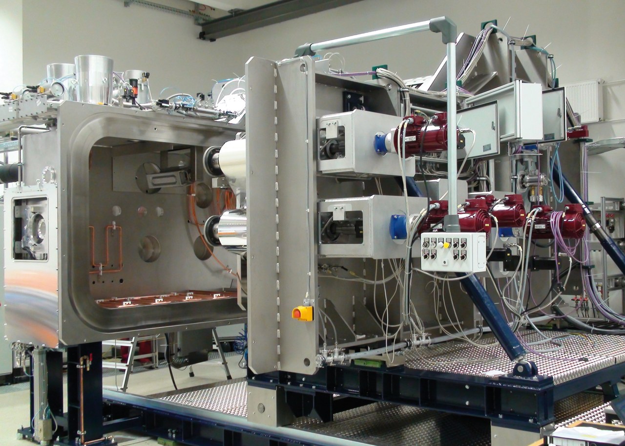
Fraunhofer FEP has huge experiences in roll-to-roll processing of OLED and offers research and development services from concept studies to sample production in the field of R2R fabrication of organic-based devices on flexible substrates for industrial partners.
Stefan Mogck, head of department roll-to-roll organic technology at Fraunhofer FEP summarizes: "We processed the OLED in vacuum in a roll-to-roll process on SEFAR TCS Planar substrates with a specific developed drying process and barrier film lamination. Altogether we deposited the OLED 30 m in length and 30 cm in width and OLED size up to 250 cm²."
About Sefar AG
Sefar AG is the leading manufacturer of precision fabrics from monofilaments for the screen printing and filtration markets. Sefar products are used in a wide variety of industries, reaching from electronics, graphics, medical, automotive, food and pharma-ceutical applications to aerospace, mining and refining, and architecture. With its profound understanding of the applications, Sefar helps its customers to achieve optimum results in their industrial processes. Subsidiaries and fabrication centers in 26 countries and on six continents provide local technical services for the broad range of solutions offered by Sefar. Sefar Group operates weaving plants in Switzerland, Romania, and Thailand. Its Monosuisse division produces fine and medium yarns in Switzerland, Poland, Romania, and Mexico. In 2015 the Sefar Group achieved sales of 282 million Swiss Francs and employed some 2,200 employees. Further information is available at www.sefar.ch or contact electrodes@sefar.com for further questions related to SEFAR TCS Planar.
About Fraunhofer FEP
The Fraunhofer Institute for Organic Electronics, Electron Beam and Plasma Technology FEP works on innovative solutions in the fields of vacuum coating, surface treatment as well as organic semiconductors. The core competences electron beam technology, sputtering and plasma-activated deposition, high-rate PECVD as well as technologies for the organic electronics and IC/system design provide a basis for these activities. Thus, Fraunhofer FEP offers a wide range of possibilities for research, development and pilot production, especially for the processing, sterilization, structuring and refining of surfaces as well as OLED microdisplays, organic and inorganic sensors, optical filters and flexible OLED lighting. Our aim is to seize the innovation potential of the electron beam, plasma technology and organic electronics for new production processes and devices and to make it available for our customers.
