NeoPac Unveiled 8 inches Wafer Level PackagingTechnology for LEDs Illumination
NeoPac Opto, Inc. a Taiwan based technology-driven LEDs lighting company recently announced its newly developed technology on 8 inches silicon-based wafer level package (WLP) for LEDs illumination, which is derived from its patented NeoPac Universal Platform (NUP) and LEDs Standard Light Sources.
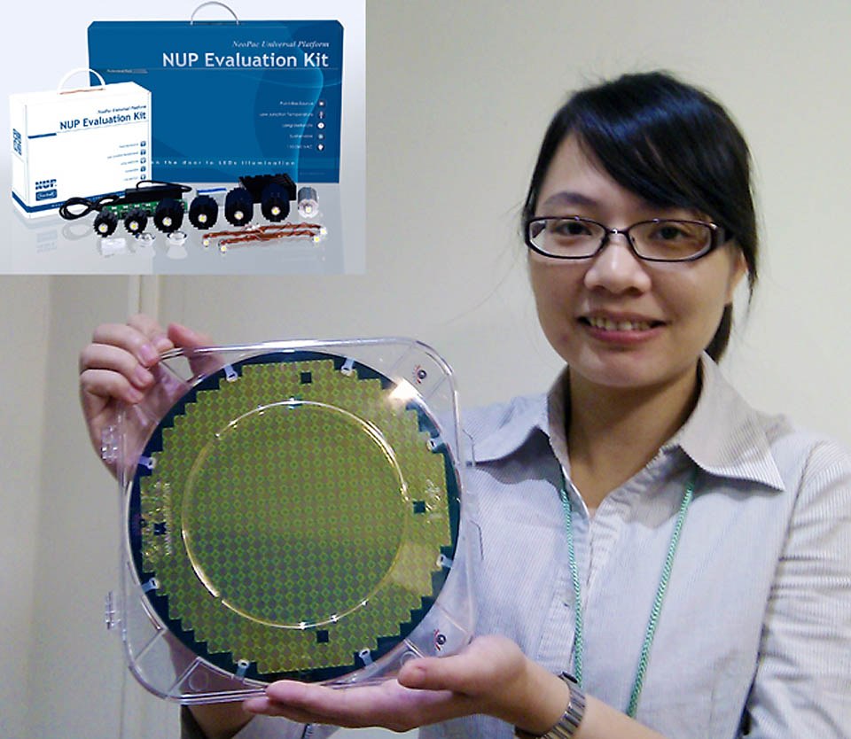
 for LEDs delivers 500,000 maintained lumens on a single 8 inches silicon wafer.")
This 8 inches semiconductor manufacturing process is for NeoPac’s unique ultra-high-power, multi-chip-module, single-packaged and point-like-source LEDs, or the so-called NeoPac Emitter. By coupling NeoPac Emitter together with its patented, highly effective micro heat pipe based heat-dissipation mechanism, a sustainable LEDs standard light source, so-called NeoPac Light Engine is available for LEDs general lighting. The integrated ultra high brightness NeoPac Light Engine is actually made by a system-in-package (SIP) approach.
LEDs WLP (Wafer-Level-Package) is a semiconductor process that LEDs chips can be directly mounted along with a phosphor coating, wire bonding, and packaging processes on a whole silicon wafer. More than 480 pcs multi-chips-module (MCM) consisting of 3,840 pcs LEDs power chips can be automatically mounted for NeoPac Emitter upon single 8 inches silicon wafer.
NeoPac plans to bring this advanced LEDs packaging technology into mass production in 2011. “The 8 inches WLP approach will drive the advancement of NeoPac’s currently far-beyond-leading technology for LEDs illumination even much ahead into a new era”, emphasized by Jeffrey Chen, Chairman and CEO of NeoPac Opto.
Each NeoPac Emitter can emit maintained lumen at 1,000 lm. Most importantly, the standard light source will suitably fit any secondary optics design for a variety of LEDs illumination applications that owing to the intrinsic merits of the lighting characteristic of point-like-source. Furthermore, the effective Useful Life (L70) of such a light engine can sustain much longer than 60,000 hours. By this new WLP manufacturing technology, it’s possible to deliver at the amount of higher than 500,000 maintained lumen on a single 8 inches silicon wafer. According to NeoPac’s sustainable technology roadmap and LEDs chips’ lumen efficacy improvement, it’s estimated that the package on the same 8 inches silicon wafer can deliver total maintained lumen output up to one million (1 M) lumen in 2 years later. This technology is about to enable the mass-production of LEDs lighting, which can substantially reduce the manufacturing cost in quantity.
The development of 8 inches WLP technology for manufacturing LEDs illumination packages which is very similar to making DRAM in semiconductor industry, again implicates that the maturity of LEDs illumination technology is about to come. “The Haitz’s law in LEDs industry for predicting lumen outputs is something like to matching into Moore’s Law in semiconductor industry”, said by Jeffrey Chen.
