Scientists Reveal the Fundamental Limitation of In Concentration in InGaN Solid-State Devices
For the first time an international research group has revealed the core mechanism that limits the indium (In) content in indium gallium nitride ((In, Ga)N) thin films - the key material for blue light emitting diodes (LED). Increasing the In content in InGaN quantum wells is the common approach to shift the emission of III-Nitride based LEDs towards the green and, in particular, red part of the optical spectrum, necessary for the modern RGB devices. The new findings answer the long-standing research question: why does this classical approach fail, when we try to obtain efficient InGaN-based green and red LEDs?
Despite the progress in the field of green LEDs and lasers, the researchers could not overcome the limit of 30% of indium content in the films. The reason for that was unclear up to now: is it a problem of finding the right growth conditions or rather a fundamental effect that cannot be overcome? Now, an international team from Germany, Poland and China has shed new light on this question and revealed the mechanism responsible for that limitation.
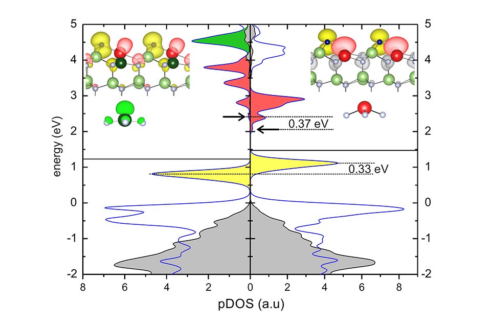
The figure above shows the on-site projected density of states (pDOS) of a 2 ×2 N adatom (0001) GaN surface with 25% InN at the topmost surface layer. (a) and (b) The In atom sits at a fourfold/triply coordinated site, respectively. The blue curves indicate the pDOS on the N adatom and on the first surface layer atoms. The gray shaded area denotes the pDOS from the fourth surface layer and the yellow shaded area the highest occupied surface state. The arrows indicate the onset of the lowest unoccupied surface states and the horizontal solid lines the position of the highest occupied states. (Insets) Yellow, red, and green colored density plots indicate the partial charge density of the states in the energy range shaded in yellow, red, and green in the pDOS, respectively. (Insets bottom) Schematic representation of the tetrahedra formed by the triply coordinated metal atoms and the three N atoms bound to them. The red/green isocontour surface shows the corresponding dangling bond state. Dark/light small balls denote the N adatom/atoms, respectively. Red/green balls are the In/Ga atoms, respectively. The dark green in the left inset denote the triply coordinated Ga atom.
In their work the scientists tried to push the indium content to the limit by growing single atomic layers of InN on GaN. However, independent on growth conditions, indium concentrations have never exceeded 25% - 30% - a clear sign of a fundamentally limiting mechanism. The researchers used advanced characterization methods, such as atomic resolution transmission electron microscope (TEM) and in-situ reflection high-energy electron diffraction (RHEED), and discovered that, as soon as the indium content reaches around 25 %, the atoms within the (In, Ga)N monolayer arrange in a regular pattern - single atomic column of In alternates with two atomic columns of Ga atoms. Comprehensive theoretical calculations revealed that the atomic ordering is induced by a particular surface reconstruction: indium atoms are bonded with four neighboring atoms, instead of expected three. This creates stronger bonds between indium and nitrogen atoms, which, on one hand, allows to use higher temperatures during the growth and provides material with better quality. On the other hand, the ordering sets the limit of the In content of 25%, which cannot be overcome under realistic growth conditions.
"Apparently, a technological bottleneck hampers all the attempts to shift the emission from the green towards the yellow and the red regions of the spectra. Therefore, new original pathways are urgently required to overcome these fundamental limitations," states Dr. Tobias Schulz, scientist at the Leibniz-Institut fuer Kristallzuechtung; "for example, growth of InGaN films on high quality InGaN pseudo-substrates that would reduce the strain in the growing layer."
However, the discovery of ordering may help to overcome well known limitations of the InGaN material system: localization of charge carriers due to fluctuations in the chemical composition of the alloy. Growing stable ordered (In, Ga)N alloys with the fixed composition at high temperatures could thus improve the optical properties of devices.
Acknowledgements:
The work is a result of a collaboration between Leibniz-Institut fuer Kristallzuechtung (Berlin, Germany), Max-Planck-Institut fuer Eisenforschung (Duesseldorf, Germany), Paul-Drude Institut fuer Festkoerperelektronik (Berlin, Germany), Institute of High-Pressure Physics (Warsaw, Poland), and State Key Laboratory of Artificial Microstructure and Mesoscopic Physics (Beijing, China).
The original paper is available at http://dx.doi.org/10.1103/PhysRevMaterials.2.011601 or https://www.researchgate.net/publication/322323121_Elastically_frustrated_rehybridization_Origin_of_chemical_order_and_compositional_limits_in_InGaN_quantum_wells
