SDK develops new crystal growth technology for GaN-based blue/white LEDs
Showa Denko K.K. (SDK) has developed a new process for making high-quality compound semiconductors based on gallium nitride (GaN) and other nitrides to meet growing demand mainly for use in blue/white LEDs.
")
")
The new process, named the “Hybrid PPDTM process,” is a combination of the conventional metal organic chemical vapor deposition (MOCVD) process and SDK’s proprietary plasma assisted physical deposition (PPDTM) process for growing nitride-based semiconductor crystals.
The new process technology enables the production of four-inch epitaxial wafers with high quality, which is not possible with the conventional MOCVD process. SDK has also succeeded, using the Hybrid PPD process, in developing blue LEDs with the highest-level brightness on the market today. SDK will start commercial shipments of these blue LEDs within this year.
Furthermore, SDK has decided to build a facility at its site in Chiba, Japan, to produce four-inch epitaxial wafers based on the new process technology. Due to the larger size of wafers under the new technology and the construction of the new line, SDK’s blue LED production capacity will be increased, from 30 million units a month at present, to 100 million units a month by the end of this year.
Under the ongoing medium-term consolidated business plan, the Passion Project, SDK is aggressively expanding its ultra bright LED business, centering on GaN-based semiconductors. SDK aims to strengthen its presence in the growing LCD backlighting and general illumination markets on the strength of the new process technology and further development of compound semiconductors of other colors and wavelengths, having still higher brightness and power.
[Outline of the new hybrid PPD process]
While GaN-based blue/white LEDs (typical nitride-based compound semiconductors) are already superior to other light sources (ex. incandescent lamp, cold-cathode tube) in terms of illuminant efficiency, there is a need for new technology for mass production of high-quality epitaxial wafers.
SDK’s new Hybrid PPD process ensures substantially higher production efficiency, enabling the manufacture of four-inch epitaxial wafers with improved crystal quality.
Meanwhile, SDK’s Hybrid PPD process, based on the epitaxial growth technology accumulated over many years, provides layers of high-quality crystals and provides higher production efficiency compared with the conventional MOCVD process. SDK has applied for more than 30 patents for the Hybrid PPD process technology.
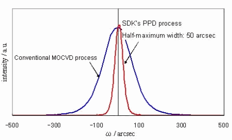
When analyzed by the X-ray rocking curve (XRC) method, the layer of single crystal nitride formed on a sapphire substrate produced by the PPD process shows significant improvement in crystal quality over a similar product produced by the MOCVD process (Chart 1).
1. Nitride-based compound semiconductors
A general name for compound semiconductors based on (Alx,Gay,In1-x-y)N. Used mainly for the production of ultraviolet/green LEDs and blue LDs. They are now attracting attention as a new material for electronic devices.
2. GaN-based LEDs
Based on different compositions, GaN-based LEDs can provide a wide range of lights from ultraviolet to green. It is possible to produce LEDs with wide-ranging wavelengths by combining ultraviolet/blue LEDs with phosphor. (Phosphor is a luminescent material that converts part of the absorbed light into emitted luminescent radiation of different wavelengths.
3. Epitaxial growth
A technology to form a semiconductor layer having the same crystalline orientation as the substrate on which it is grown.
For further information, contact:
IR & PR Office (Phone: 81-3-5470-3235)
