Using Nanostructures to Improve LED Light Emission
Application of nanosphere lithography to create uniform surface roughness on an optical device sample promotes light extraction and collection efficiency. In recent years, nanopattern definition has become a subject of extensive exploration owing to its ability to improve device performance in electronics and optoelectronics. The literature proposes a variety of techniques, including electron-beam lithography, which gives uniform nanopatterns but is expensive, and self-assembled metal nanomasks, which scatter nonuniformly on the sample. As an alternative, we have developed a technology called nanosphere lithography that creates nanopatterns by spin-coating a monolayer of nanospheres on top of the device surface. We have used the technology to fabricate nanopatterns on gallium nitride (GaN)-based LEDs to improve light extraction and collection efficiency.

 The nanospheres are first spin-coated onto the sample, followed by dry etching to define patterns. (b) The silica spheres and protection layer are then removed. The device-fabrication process is completed following deposition of contact metal. (c) Structure of an LED equipped with nanorod reflectors.")
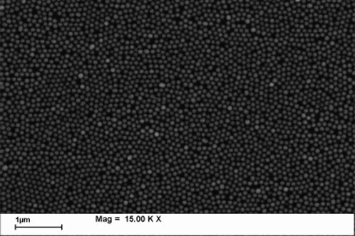
Nanopatterns are defined by spin-coating nanospheres on the entire sample. The diameters of the nanospheres range from several nanometers to microns depending on the type. In our work, we chose silica particles. The particles were self-organized and firmly bound to the substrate surface by van der Waals (weak electronic) forces when the spin condition and nanosphere solvent are properly adjusted (see Figure 1). We then dry-etched the sample to form nanopatterns using the nanospheres as a hard mask, after which we removed them. Generally, nanorod distribution is determined by the spin speed and the silica nanosphere concentration in the solvent.
Nanosphere lithography can be applied to create uniform surface roughness on the LED samples, which improves light extraction.1 The large refractive index difference between air and semiconductor (for example, 2.5 for GaN) means that the critical angle for photons to escape from the LED is very small (23° for a GaN/air interface). Thus, external extraction efficiency is one of the major bottlenecks for LEDs. In nanosphere lithography, the photons are scattered, and consequently the chance of an electron falling within the escape cone is increased. In our experiment, we achieved surface roughness all over the 2-inch wafer with nanosphere spin casting and inductively coupled plasma dry etching. With nanopatterns on the p-doped GaN surface, we observed an ~40% increase of output power at 20mA injection current compared with conventional LEDs with a flat semiconductor-air interface, proving the effectiveness of light extraction. A similar approach can be used to roughen the transparent conducting layer, which leads to an ~25% output-power enhancement (see Figure 2).
In addition, nanosphere lithography can be used to fabricate nanorods by etching the sample further through the p-i-n structure using nanospheres as the etch mask. Applying this approach, we demonstrated a new device whose LEDs were embedded with nanorod reflectors.2 In the past, most work on LED power enhancement focused on extracting light vertically. Even though lateral guided modes fall within the critical angle of total internal reflection when propagating toward the mesa sidewall, they are unfavorable since only a small amount of extracted light contributes to the designated radiation angle through sidewall scattering. The use of lateral guided modes (i.e., horizontally propagated light) that are extracted from the mesa sidewalls has rarely been addressed. We fabricated such a reflector structure and found that it enhances power output. A device equipped with nanorod arrays 20μm wide showed an ~25% increase in light collection compared with conventional LEDs (i.e., without nanorod sidewall reflectors). The results establish that this configuration enables emission to be scattered, reflected, or diffracted to the surface normal.
In summary, using the nanosphere approach, we have been able to realize nanopatterns on optical devices at very low cost. Moreover, nanopatterns improve device performance. As a next step, we plan to fabricate GaN nanorod LED arrays with a diameter smaller than the average distance between defects. By reducing contact resistance, we expect the device to show high emission density for potential next-generation lighting.
The research work was conducted by Min-Yung Ke and Yun-Wei Cheng under the supervision of JianJang Huang at the Graduate Institute of Photonics and Optoelectronics, National Taiwan University. JianJang Huang's group focuses on applying nanotechnology to optoelectronics and electronics.
About the Author:
JianJang Huang, Min-Yung Ke, Yun-Wei Cheng
Graduate Institute of Photonics and Optoelectronics
National Taiwan University
Taipei City, Taiwan
JianJang Huang received his PhD from the University of Illinois, Urbana-Champaign (2002), and is currently an associate professor. His research focuses on the application of nanostructures to electronic and optoelectronic devices.
Min-Yung Ke received his PhD from the Graduate Institute of Photonics and Optoelectronics, National Taiwan University (2010). His research interest is zinc oxide-based light-emitting nanostructures. He will join the Taiwan Semiconductor Manufacturing Company in September 2010.
Yun-Wei Cheng is currently pursuing his PhD under the supervision of JianJang Huang. His research interest focuses on applying nanorod structures to LEDs.
References:
1. Min-Yann Hsieh, Cheng-Yin Wang, Liang-Yi Chen, Tzu-Pu Lin, Min-Yung Ke, Yun-Wei Cheng, Yi-Cheng Yu, Improvement of external extraction efficiency in GaN-based LEDs by SiO2 nanosphere lithography, IEEE Electron Device Lett. 29, pp. 658-660, 2008.
2. Yun-Wei Cheng, Kun-Mao Pan, Cheng-Yin Wang, Hung-Hsien Chen, Min-Yung Ke, Cheng-Pin Chen, Min-Yann Hsieh, Han-Ming Wu, Lung-Han Peng, JianJang Huang, Enhanced light collection of GaN light emitting devices by redirecting the lateral emission using nanorod reflectors, Nanotechnology 20, pp. 035202, 2009.
