Light emitting diode package having multiple molding resins
Disclosed is a light emitting diode (LED) package having multiple molding resins. The LED package includes a pair of lead terminals. At least portions of the pair of lead terminals are embedded in a package main body. The package main body has an opening through which the pair of lead terminals is exposed. An LED die is mounted in the opening and electrically connected to the pair of lead terminals. A first molding resin covers the LED die. A second molding resin with higher hardness than the first molding resin covers the first molding resin. Therefore, stress to be imposed on the LED die can be reduced and the deformation of the molding resins can be prevented.

Background of the invention
[0007] [2] In general, a light emitting diode (LED) package includes a molding resin for covering a mounted LED die. The molding resin protects the LED die from the external environment. That is, the molding resin protects the LED die and the bonding wire from the external force and prevents the damage of the LED die by blocking moisture from the atmosphere. In addition, the molding resin may contain a phosphor that can change the wavelength of light emitted from the LED die. As the result, a white light can be obtained using an LED die from which an ultraviolet or blue light is emitted.
[0008] [3] Furthermore, the LED die generates heat when emitting light. The heat is transferred to the surroundings of the LED die. Thus, the molding resin covering the LED die undergoes a thermal cycle due to the repeated operation of the LED die. In a case where the molding resin has higher hardness, the molding resin may be cracked or peeled during the thermal cycle. In addition, the LED die may be broken or the bonding wire may be cut, due to thermal stress caused by a difference between thermal expansion coefficients of the molding resin and the LED die. The cracking and peeling of the molding resin lead to non-uniformity of the emitted light and deteriorates a moisture resistance characteristic. Moreover, in a case where the molding resin is formed of a thermoplastic resin, the residual stress after the curing is large, and thus, the aforementioned problem becomes worse.
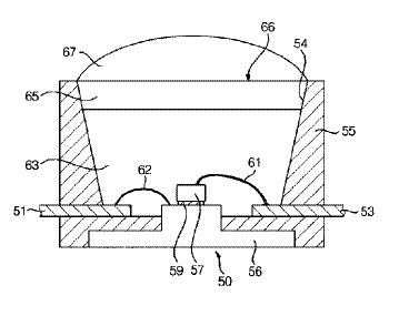
[0009] [4] An LED package capable of preventing the cracking and peeling of a molding resin due to a thermal cycle is disclosed in U.S. Patent No. 6,747,293 (Nitta, et al.) entitled Light emitting device. Fig. 1 is a sectional view showing an LED package 500 disclosed in the above 293 patent.
[0010] [5] Referring to Fig. 1, the LED package 500 includes lead terminals 501 and 502 formed out of a lead frame and a main body 503 formed integrally with the lead terminals. The main body 503 is made of a thermoplastic resin. The lead terminals 501 and 502 are disposed in such a way that one ends thereof face each other and the other ends thereof extend in opposite directions to project from the main body 503 to the outside.
[0011] [6] In the meantime, the main body 503 has an opening 505 and an LED die 506 is mounted on a bottom surface of the opening. The LED die 506 may be attached on one lead terminal 501 using a conductive adhesive 507 and connected to the other lead terminal 502 through a bonding wire 509. The opening 505 has an inclined inner wall 504 such that light emitted from the LED die 506 can be reflected to the outside.
[0012] [7] A sealing resin 511 is disposed within the opening 505 in such a manner as to cover the top of the LED die 506. The sealing resin 511 is a silicone resin having a relatively high hardness of 50 to 90 in JISA of Japanese Industrial Standards (JIS). A lens 513 is provided above the sealing resin 511 to collect light.
[0013] [8] The sealing resin 511 of the LED package 500 has lower hardness than an epoxy resin having a hardness of 95 in JISA and thus the cracking or peeling of the sealing resin can be prevented. In addition, since the sealing resin 511 of the LED package 500 has a relatively higher hardness as compared with a silicone resin having a hardness of 30 to 40 in JISA, the external force has less influence on the LED die 506. However, since the sealing resin 511 of the LED package 500 has a relatively higher hardness as compared with the silicone resin, it causes a relatively larger amount of residual stress when cured. Further, relatively higher thermal stress is generated due to a thermal cycle. In particular, in a case where the size of the opening or the input power increases, the above stress increases further, thereby reducing the reliability of the LED die 506 and causing the bonding wire 507 to be cut.
[0014] [9] Meanwhile, the luminous power of an LED is substantially proportional to the input power. Therefore, high luminous power can be obtained by increasing the electric power input to the LED. However, the increase of the input power results in the increase of the junction temperature of the LED. The increase of the junction temperature of an LED causes the loss of photometric efficiency which represents the conversion rate of input energy into visible light. Therefore, it is required to prevent the junction temperature of the LED from rising due to the increased input power.
[0015] [10] An example of an LED package that employs a heat sink to prevent the increase of the LED junction temperature is disclosed in U.S. Patent No. 6,274,924Bl, entitled Surface mountable LED package. As described in the 924 patent, the LED die is thermally coupled on the heat sink and thus can be maintained to a lower junction temperature. Therefore, a relatively higher input power can be supplied to the LED die to obtain higher luminous power.
[0016] [11] In this conventional LED package, however, the heat sink can be easily separated from the package main body, which results in structural instability. When the heat sink is separated from the package main body, bonding wires that electrically connect the LED die mounted onto the heat sink with the leads are cut off to bring an irreparable damage to the LED package. Thus, there is a need to provide an LED package in which the heat sink can be prevented from being separated from the package main body.
Brief summary of the invention
The present invention relates to a light emitting diode package having a molding resin, and more particularly, to a light emitting diode package, in which a light emitting diode die is covered with a molding resin having lower hardness and then with another molding resin having higher hardness in order to alleviate stress imposed on the light emitting diode die and to prevent the deformation of a top surface of the molding resin.
Claims
[1] A light emitting diode package having multiple molding resins, comprising: at least a pair of lead terminals; a package main body having an opening exposing the pair of lead terminals, the package main body embedding at least a portion of the pair of lead terminals; a light emitting diode die mounted in the opening and electrically connected to the pair of lead terminals; a first molding resin covering the light emitting diode die; and a second molding resin covering the first molding resin and having higher hardness than the first molding resin.
[2] The light emitting diode package as claimed in claim 1, wherein the first molding resin has a Durometer Shore value of less than 50A and the second molding resin has a Durometer Shore value of no less than 50A.
[3] The light emitting diode package as claimed in claim 2, wherein the first and second molding resins are formed of an epoxy or silicone resin. [4] The light emitting diode package as claimed in claim 3, wherein the second molding resin is formed in the shape of a lens.
[5] The light emitting diode package as claimed in claim 3, wherein the first and/or second molding resin contains a phosphor.
[6] The light emitting diode package as claimed in claim 1, further comprising a heat sink coupled to the bottom of the package main body and partially exposed through the opening, wherein the light emitting diode die is mounted on a top surface of the heat sink.
[7] The light emitting diode package as claimed in claim 6, wherein the heat sink has a base and a protrusion projecting upward from the center portion of the base.
[8] The light emitting diode package as claimed in claim 7, wherein the heat sink is formed with a latching step on at least one of sides of the base and/or the protrusion.
[9] A light emitting diode package having multiple molding resins, comprising: a heat sink support ring; a heat sink inserted into the support ring; at least two lead terminals disposed at both sides of the support ring and spaced apart from the support ring and heat sink; a package main body molded with the heat sink and lead terminals to support the heat sink and lead terminals, the package main body having an opening through which the upper end of the heat sink and portions of the lead terminals are exposed; at least a light emitting diode die mounted on a top surface of the heat sink; bonding wires for electrically connecting the light emitting diode die and lead terminals; a first molding resin covering the light emitting diode die; and a second molding resin covering the first molding resin and having higher hardness than the first molding resin.
[10] The light emitting diode package as claimed in claim 9, wherein the first molding resin has a Durometer Shore value of less than 50A and the second molding resin has a Durometer Shore value of no less than 50A.
[11] The light emitting diode package as claimed in claim 10, wherein the first and second molding resins are formed of an epoxy or silicone resin.
[12] The light emitting diode package as claimed in claim 11, wherein the second molding resin is formed in the shape of a lens.
[13] The light emitting diode package as claimed in claim 9, wherein the heat sink has a base and a protrusion projecting upward from the center portion of the base and inserted into the support ring.
[14] The light emitting diode package as claimed in claim 13, wherein the heat sink is further formed with a support ring receiving groove at a side of the protrusion to receive the support ring.
[15] The light emitting diode package as claimed in claim 9, wherein the package main body is formed of a thermosetting resin or a thermoplastic resin by insert molding the lead terminals and heat sink.
See full document in pdf.
