Light emitting diode package with protective function against electrostatic discharge
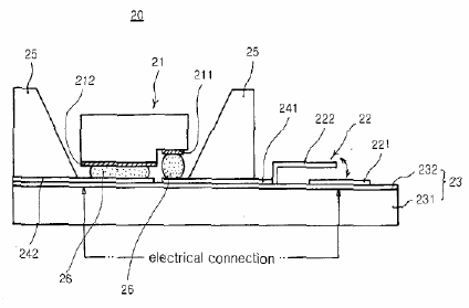
The present invention provides an LED package having an MEMS switch operated by electrostatic force, capable of continuously protecting an LED from excessive current due to electrostatic discharge. The invention includes a submount with first and second electrode patterns formed thereon; an LED mounted on the submount, having an n-electrode electrically connected to the first electrode pattern and a p-electrode electrically connected to the second electrode pattern; and an MEMS switch including a first conductive plate and a second conductive plate bent to have an area over and vertically apart from the first conductive plate, wherein the first and second conductive plates are electrically connected to the first and second electrode patterns, and the second conductive plate comes in contact with the first conductive plate by electrostatic force upon being applied with voltage higher than a predetermined level of voltage.


Background of the invention
[0002] 1. Field of the Invention
[0003] The present invention relates to a Light Emitting Diode (LED) package capable of preventing damage to an LED due to electrostatic discharge, and more particularly, to an LED package having a protective function against electrostatic discharge, in which a Micro Electro Mechanical Systems (MEMS) switch operable to electrostatic force is provided to continuously protect an LED from excessive current due to electrostatic discharge.
[0004] 2. Description of the Related Art
[0005] Having superior physical and chemical properties, a nitride semiconductor using nitride such as GaN has become popular as core material for photoelectric material and electric devices recently. Particularly, the nitride semiconductor light emitting device is capable of generating a range of light including green, blue and ultraviolet ranges, and with its luminance rapidly enhanced by the recent technological development, it has been extensively applied to the fields such as all-natural color electric bulletin boards and illumination apparatuses.
[0006] In general, a nitride semiconductor light emitting device has a disadvantage in that it is very vulnerable to static electricity compared with the semiconductors composed of other compounds such as GaP or GaAlAs. For example, the nitride semiconductor light emitting device can be destroyed by constant voltage in forward direction of about hundreds of volts (100V or higher), and also by constant voltage in backward direction of about tens of volts (30V or higher). Such vulnerability to constant voltage can be a cause of damage to the LED when handling the nitride semiconductor light emitting device. Therefore, various researches have been conducted to overcome the vulnerability of the nitride semiconductor light emitting device to static electricity. In relation to this, U.S. Pat. No. 6,861,677 (entitled "Package of Light Emitting Diode with Protective Element," assigned to United Epitaxy Co., Ltd.) discloses an LED package having a combined structure of a nitride semiconductor light emitting device and a Zener diode on a single substrate.
[0007] FIG. 1(a) illustrates the conventional LED package disclosed in U.S. Pat. No. 6,861,677. With reference to FIG. 1(a), in the LED package 10 disclosed in U.S. Pat. No. 6,861,677, an n-electrode 111 is connected to a p-electrode 121 of the Zener diode 13 through a conductive bump 151, and a p-electrode 112 of an LED 11 is connected to a conductive heat-radiation structure 14 through another conductive bump 152, and the conductive heat-radiation structure 14 and the n-electrode of the Zener Diode 12 are adhered to a substrate 13 for electrical connection.
[0008] The structure of the conventional LED package 10 described above has a circuit structure as shown in FIG. 1(b). That is, an anode of the LED 11 is connected to a cathode of the Zener diode 12, and a cathode of the LED 11 is connected to an anode of the Zener diode 12 in parallel. Therefore, when both electrodes of the LED 11 are applied with backward voltage, then the Zener diode 12 becomes applied with forward voltage, thereby current runs through the Zener diode 12, not through the LED 11. In addition, in case when forward voltage is applied to both electrodes of the LED, if voltage lower than the breakdown voltage of the Zener diode 12 is applied, current runs through the LED 11, and light emission takes place. If forward voltage higher than the breakdown voltage of the Zener diode 12 is applied, the Zener diode 12 breaks down, allowing all currents to run through the Zener diode 12. Therefore, the conventional LED package uses the Zener diode 12 to prevent current by excessive voltage applied forward and backward by static electricity from running through the LED 11, thereby preventing damage to the LED due to static electricity.
[0009] However, the conventional LED package which protects the LED from electrostatic discharge uses the Zener diode 11, and thus once excessive current has run through the Zener diode 11, the Zener diode 11 can no longer be operated, no longer performing the protective function against electrostatic discharge. In other words, the conventional LED package having a protective function against electrostatic discharge can perform the protection function only once, and cannot perform repeatedly, and thus the LED remains vulnerable to the exposure to excessive current due to electrostatic discharge.
Brief summary of the invention
[0010] The present invention has been made to solve the foregoing problems of the prior art and it is therefore an object of the present invention to provide an LED package capable of continuously protecting an LED from excessive current due to electrostatic discharge. [0011] According to an aspect of the invention for realizing the object, there is provided a Light Emitting Diode (LED) package having a protective function from electrostatic discharge comprising: a submount with first and second electrode patterns formed thereon; an LED mounted on the submount, having an n-electrode electrically connected to the first electrode pattern and a p-electrode electrically connected to the second electrode pattern; and an MEMS switch including a first conductive plate disposed on the submount and a second conductive plate disposed apart from the first conductive plate on the submount and bent to have an area over and vertically apart from the first conductive plate, wherein the first conductive plate is electrically connected to one of the first and second electrode patterns, and the second conductive plate is electrically connected to the other electrode pattern, and the second conductive plate comes in contact with the first conductive plate by electrostatic force upon being applied with voltage higher than a predetermined level of voltage. [0012] In a preferred embodiment of the present invention, the submount comprises a silicon substrate and a SiO2 film formed on the silicon substrate. Using the silicon substrate for the submount allows application of Micro Electro Mechanical System (MEMS) process, thereby allowing integral formation of MEMS switch with the submount without additional step of separately producing the MEMS switch to attach on the submount. That is, in case of using the silicon substrate for the submount, the first and second conductive plates may be integrally formed with the submount. In the mean time, since a silicon substrate is conductive, it is preferable to form a SiO2 film on the silicon substrate to form a plurality of electrodes necessary for electrical insulation.
[0013] In an embodiment of the present invention, in order to electrically connect the two conductive plates with the first and second electrode patterns, the submount may further comprise conductive patterns formed on the submount, electrically connecting the first conductive plate to one of the first and second electrode patterns and electrically connecting the second conductive plate to the other electrode pattern.
[0014] In an embodiment of the present invention, it is preferable that the first and second conductive plates are made of metal, and particularly preferable made of Al. In addition, the resilient second conductive plate may be made of poly-silicon. It is preferable that the predetermined level of voltage that makes the first conductive plate and the second conductive plate come in contact with each other by electrostatic force is up to 30V.
[0015] In addition, an embodiment of the present invention may further comprise a reflector formed around the LED on the submount for reflecting the light emitted from the LED upward.
Claims
1. A Light Emitting Diode (LED) package having a protective function against electrostatic discharge comprising:
a submount with first and second electrode patterns formed thereon;
an LED mounted on the submount, having an n-electrode electrically connected to the first electrode pattern and a p-electrode electrically connected to the second electrode pattern; and
an MEMS switch including a first conductive plate disposed on the submount and a second conductive plate disposed apart from the first conductive plate on the submount and bent to have an area over and vertically apart from the first conductive plate, wherein the first conductive plate is electrically connected to one of the first and second electrode patterns, and the second conductive plate is electrically connected to the other electrode pattern, and the second conductive plate comes in contact with the first conductive plate by electrostatic force upon being applied with voltage higher than a predetermined level of voltage.
2. The LED package according to claim 1, wherein the submount comprises a silicon substrate and a SiO2 film formed on the silicon substrate.
3. The LED package according to claim 2, wherein the first and second conductive plates are integrally formed with the submount, and electrically connected to the first and second electrode patterns, conductive patterns on the submount, respectively.
4. The LED package according to claim 1 or 3, wherein the submount further comprises conductive patterns formed on the submount, electrically connecting the first conductive plate to one of the first and second electrode patterns and electrically connecting the second conductive plate to the other electrode pattern.
5. The LED package according to claim 1, wherein the first and second conductive plates are made of metal.
6. The LED package according to claim 5, wherein the first and second conductive plates are made of Al.
7. The LED package having according to claim 1, wherein the second conductive plate is made of poly-silicon.
8. The LED package according to claim 1, wherein the predetermined level of voltage is up to 30V.
9. The LED package according to claim 1, further comprising a reflector formed around the LED on the submount for reflecting the light emitted from the LED upward.
See full document in pdf.
