Semiconductor light emitting diode having textured structure and method of manufacturing the same
A semiconductor light emitting diode having a textured structure and a method of manufacturing the semiconductor light emitting diode are provided. The method includes forming a first semiconductor layer on a substrate; forming a textured structured first semiconductor layer by penetrating a material of a material layer into the first semiconductor layer after the material layer is formed on the first semiconductor layer and annealed; and forming a second semiconductor layer on the first semiconductor layer.

Background of the invention
[0001] The present invention relates to a semiconductor light emitting diode, and more particularly, to a semiconductor light emitting diode having a textured structure to improve light extraction efficiency and a method of manufacturing the same.
[0002] A light emitting diode (LED) is a device used for converting electrical energy into infra red rays, visible tight, or other light using the characteristics of a compound semiconductor. The light emitting diode is a kind of electro luminescent (EL) device, and presently, the light emitting diodes that employ an III-V group compound semiconductor are practically used.
[0003] The III-V group compound semiconductor is a direct transition type semiconductor, and is widely used for LEDs or laser diodes (LDs) since it provides stable operation at a higher temperature than devices that use other semiconductors. The III-V group compound semiconductor is typically formed on a substrate formed of sapphire Al2O3 or SiC. To improve light emission efficiency, or light extraction efficiency, LEDs having a variety of structures have been studied. Current studies use a textured structure on a light extraction region of the LED to improve the light extraction efficiency.
[0004] At an interface between material layers having different refractive indexes, the passing of light is interrupted by different refractive indexes of the material layers. In the case of a flat interface, when light passes from a semiconductor layer having a greater refractive index (n=2.5) into an air layer having a smaller refractive index (n=1), the light must enter the flat interface at less than a predetermined angle with respect to the normal to the flat surface. If the light enters at an angle greater than the predetermined angle, the light totally internally reflects at the flat interface, thereby greatly reducing the light extraction efficiency. To avoid the total internal reflection of light, a method of incorporating a textured structure at the interface has been attempted.
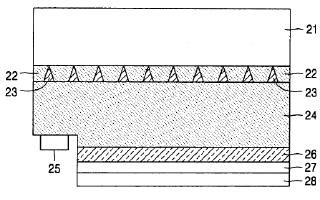
[0005] FIGS. 1A and 1B are cross-sectional views illustrating a conventional light emitting diode having a textured structure. Referring to FIG. 1A, a p-GaN layer 102, an active layer 103, an n-GaN layer 104 are sequentially formed on a p-electrode 101, and an n-electrode 105 is formed on the n-GaN layer 104. When light generated by the active layer 103 is extracted upward through the n-GaN layer 104, a textured structure 106 is incorporated at an interface between the n-GaN layer 104 and the air layer to change the incidence angle of the light.
[0006] Referring to FIG. 1 B, an n-GaN layer 112 is formed on a sapphire substrate 111, and an n-AlGaN layer 113, an active layer 114, a p-AlGaN layer 115, a p-GaN layer 116, and a p-electrode 117 are sequentially formed on a region of the n-GaN layer 112. An n-electrode 118 is formed on a region of the n-GaN layer 112 where the n-AlGaN layer 113 is not formed. This is a flip-chip structure in which light generated by the active layer 114 is mainly extracted through the transparent sapphire substrate 111. Here, the light extraction efficiency is improved by forming a textured structure 120 on the surface of the sapphire substrate 111.
[0007] A conventional semiconductor light emitting diode incorporates the textured structure 120 to improve the light extraction efficiency. However, particularly as depicted in FIG. 1 B, when the textured structure 120 is incorporated by patterning the sapphire substrate 111, the growth of a uniform semiconductor layer on the sapphire substrate 111 is difficult because the unmatched crystal structure between the sapphire substrate 111 and the semiconductor layer is likely to cause defects in the semiconductor layer, thereby reducing the light extraction efficiency.
Brief summary of the invention
[0008] The present invention provides a semiconductor light emitting diode having a structure that can increase light extraction efficiency and reduce inter crystal defects of the semiconductor light emitting diode and a method of manufacturing the same.
[0009] According to an aspect of the present invention, there is provided a method of manufacturing a semiconductor light emitting diode, comprising: forming a first semiconductor layer on a substrate; forming a textured structure first semiconductor layer by penetrating a material of a material layer into the first semiconductor layer after the material layer is formed on the first semiconductor layer and annealed; and forming a second semiconductor layer on the first semiconductor layer.
[0010] The forming of a textured structured first semiconductor layer may comprise: forming a first material layer on the first semiconductor layer; forming a second material layer on the first material layer; and annealing to cause the materials of the first and second material layers to penetrate into the first semiconductor layer.
[0011] The first material layer may be formed of a material including one of Ni and Pd.
[0012] The second material layer may be formed of a material including one of Ag and Au.
[0013] The method may further comprise etching the first semiconductor layer to remove Au from the first semiconductor layer using aqua regia , after the materials of the first material layer and the second material layer have penetrated into the first semiconductor layer.
[0014] The forming of a textured structured first semiconductor layer may comprise annealing to cause the material layers to penetrate into defected regions of the first semiconductor layer after the material layers are formed.
[0015] The method may further comprise removing the material penetrated into the first semiconductor layer from the first semiconductor layer, depositing one of SiO2 and SiN on the first semiconductor layer, and leaving SiO2 or SiN only in the textured structure of the first semiconductor layer by treating a surface of the first semiconductor layer.
[0016] The annealing may be performed under a nitrogen atmosphere.
[0017] The method may further comprise annealing under an oxygen atmosphere after annealing under the nitrogen atmosphere.
[0018] The first semiconductor layer may be formed of a compound having a formula InxAlyGa1-x-y N1-x-y(0 x 1, 0 y 1, x+y 1) undoped, doped with an n-type dopant, or doped with a p-type dopant.
[0019] The first semiconductor layer may have a thickness of 10nm to 5 m.
[0020] According to another aspect of the present invention, there is provided a semiconductor light emitting diode comprising: a first semiconductor layer formed in a textured structure; a material region which is formed between the textured structures of the first semiconductor layer and includes at least one metal selected from Ni, Pd, Au, and Ag; and a second semiconductor layer, an active layer, and a third semiconductor layer sequentially formed on the first semiconductor layer and the intermediate layer.
[0021] The first semiconductor layer may be formed of a compound having a formula InxAlyGa1-x-y N1-x-y(0 x 1, 0 y 1, x+y 1) undoped, doped with an n-type dopant, or doped with a p-type dopant.
[0022] The first semiconductor layer may have a thickness of 10nm to 5 m.
Claims
1. A method of manufacturing a semiconductor light emitting diode, comprising:
forming a first semiconductor layer on a substrate;
forming a textured structure first semiconductor layer by penetrating a material of a material layer into the first semiconductor layer after the material layer is formed on the first semiconductor layer and annealed; and
forming a second semiconductor layer on the first semiconductor layer.
2. The method of claim 1, wherein the forming of the textured structured first semiconductor layer comprises:
forming a first material layer on the first semiconductor layer;
forming a second material layer on the first material layer; and
annealing to cause the first and second material layers to penetrate into the first semiconductor layer.
3. The method of claim 2, wherein the first material layer is formed of one selected from Ni and Pd.
4. The method of claim 2, wherein the second material layer is formed of one selected from Ag and Au.
5. The method of claim 4, further comprising etching the first semiconductor layer to remove Au from the first semiconductor layer using aqua regia after the materials of the first material layer and the second material layer have penetrated into the first semiconductor layer.
6. The method of any of claims 2 to 5, wherein the forming of a textured structured first semiconductor layer comprises annealing to cause the material layers to penetrate into a defect region of the first semiconductor layer after the material layers are formed.
7. The method of claim 6, further comprising removing the material penetrated into the first semiconductor layer from the first semiconductor layer, depositing one of SiO2 and SiN on the first semiconductor layer, and leaving SiO2 or SiN only in the textured structure of the first semiconductor layer by treating a surface of the first semiconductor layer.
8. The method of claim 6 or 7, wherein the annealing is performed under a nitrogen atmosphere.
9. The method of claim 8, further comprising annealing under an oxygen atmosphere after annealing under the nitrogen atmosphere.
10. The method of any preceding claim, wherein the first semiconductor layer is formed of a compound having a formula InxAlyGa1-x-y N1-x-y(0 x 1, 0 y 1, x+y 1) undoped, doped with an n-type dopant, or doped with a p-type dopant.
11. The method of any preceding claim, wherein the first semiconductor layer has a thickness of 10nm to 5 m.
12. A semiconductor light emitting diode comprising:
a first semiconductor layer formed in a textured structure;
a material region which is formed between the textured structures of the first semiconductor layer and includes at least one metal selected from Ni, Pd, Au, and Ag; and
a second semiconductor layer, an active layer, and a third semiconductor layer sequentially formed on the first semiconductor layer and the intermediate layer.
13. The semiconductor light emitting diode of claim 12, wherein the first semiconductor layer is formed of a compound having a formula lnxAlyGa1-x-y N1-x-y (0 x 1, 0 y 1, x+y 1), undoped, doped with an n-type dopant, or doped with a p-type dopant.
14. The semiconductor light emitting diode of claim 12 or 13, wherein the first semiconductor layer has a thickness of 10nm to 5 m.
See full document in pdf.
