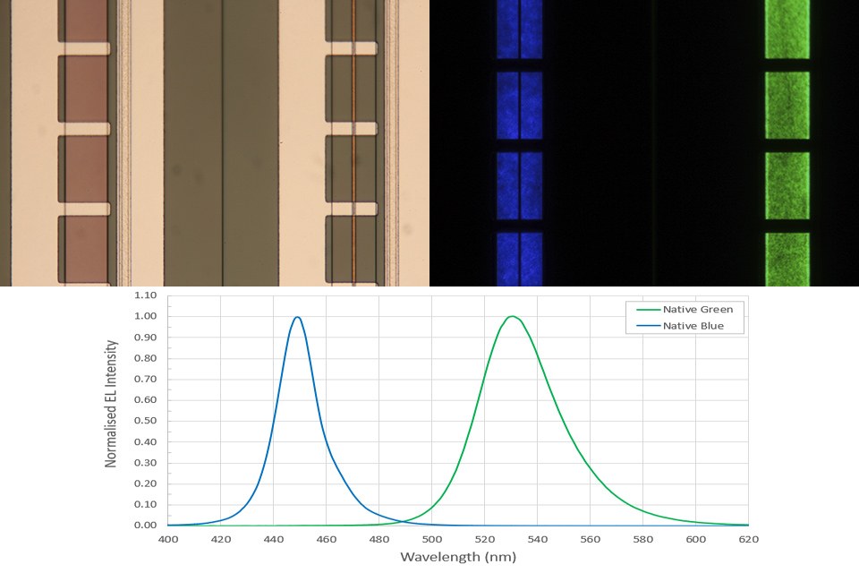
Plessey - Native Blue and Native Green Emission microLEDs from the same Wafer
Plessey, an embedded technologies developer at the forefront of microLED technology for augmented and mixed reality (AR/MR) display applications has extended the capability of their proprietary GaN-on-Silicon process to enable Native Blue and Native Green emission from the same wafer.
The potential of microLEDs is well known but several challenges remain before ramping up to large scale consumer applications. To form RGB microLED displays, typical approaches are to use a pick and place process to transfer discrete R, G and B pixels or to use Native Blue LEDs as the light source for subsequent colour conversion, to Red and Green.
Plessey's latest patented growth approach creates both Native Blue and Native Green emission layers on the same wafer. The monolithic formation of two colours significantly simplifies display manufacture. Green microLEDs have high efficiency with a narrow spectral width resulting in an excellent colour gamut when operating alongside the high performance Blue microLEDs. Plessey's new approach forms microLEDs that exhibit high current density operation and long operational lifetime.
The monolithic integration of both the native Blue and Green microLEDs on the same Silicon substrate is the result of a concerted effort aimed at solving several challenges previously considered insurmountable. Among the issues preventing the integration of multiple wavelength diode junctions are, firstly, a magnesium memory effect and diffusion from the p-type cladding of the lower junction into the upper junction.
An additional process challenge to the integration of Blue and Green microLEDs is the precise tuning of the thermal budget during the growth of the second junction to prevent indium phase separation in the blue active region. Plessey has precisely engineered the thermal budget to maintain high efficiency (IQE), low defectivity and high electrical conductivity required for high brightness display applications.
A final operation in the formation of GaN microLEDs is a post growth treatment aimed at removing hydrogen atoms that would otherwise compromise the conductivity of p-type layers. The presence of a second junction complicates the removal of hydrogen from the buried device structure negating the effect of standard post-growth activation treatments.
Plessey has successfully overcome all these challenges and created a monolithic Blue and Green microLED fabrication process that integrates these junctions vertically separated by a sub-micron layer thickness and results in very reproducible and stable diode performance, well beyond what is typical in the LED industry.
Dr Wei Sin Tan, Director of Epitaxy and Advanced Product Development, at Plessey, said:
"Our latest breakthrough has a multiplier effect on our previous successes with high efficiency monolithic native blue arrays, native green arrays and hybrid bonding to backplane by demonstrating a way to synthesize the best of our know-how into a single die.
This has enormous implications and will open the doors towards new innovations across a wide range of display applications. For mobile and large displays, a high efficiency single RGB tile can now be used for mass-transfer and for micro-displays, this creates a path to the elusive single RGB panel ultra-high resolution microLED AR display. This new process paves the way to commercial, high-performance microLED displays, bringing mass adoption of microLEDs in displays ever closer to reality.
Our achievement demonstrates once more the ability of the engineering team at Plessey to lead in the microLED technology space and deliver truly innovative solutions to well-known problems"
MicroLED technology is continuing to emerge as the most likely successor to today's smart high-performance display applications, making displays with smaller form factor, even brighter and more power efficient than current display technologies available.
Other recent ground-breaking milestones from Plessey includes the world's first wafer level bonded monolithic 3000 ppi GaN-on-silicon microLED emissive display hybridised to an active matrix CMOS backplane, and a high efficiency Native Green technology. Plessey are continuing to rapidly develop microLED display solutions with their roadmap including the production of full RGB microLED displays by 2020.
To learn more about Plessey's microLED technology, please visit plesseysemiconductors.com/products/microleds/ or contact Plessey at microleds@plesseysemi.com
About Plessey:
Plessey is an award-winning provider of full-field emissive microLED displays that combine very high-density RGB pixel arrays with high-performance CMOS backplanes to produce very high-brightness, low-power and high-frame-rate image sources for head-mounted displays (HMDs), and augmented reality (AR) and virtual reality (VR) systems. Plessey operates leading-edge 150mm and 200mm wafer processing facilities to undertake design, test and assembly of LED products, and a comprehensive suite of photonic characterization and applications laboratories. For more information, visit Plessey's website at plesseysemiconductors.com/

